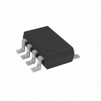
AD5227BUJZ10-R2 Analog Devices Inc, AD5227BUJZ10-R2 Datasheet - Page 6

AD5227BUJZ10-R2
Manufacturer Part Number
AD5227BUJZ10-R2
Description
IC DGTL POT 10K UP/DN TSOT23-8
Manufacturer
Analog Devices Inc
Datasheet
1.AD5227BUJZ10-RL7.pdf
(16 pages)
Specifications of AD5227BUJZ10-R2
Taps
64
Resistance (ohms)
10K
Number Of Circuits
1
Temperature Coefficient
35 ppm/°C Typical
Memory Type
Volatile
Interface
Up/Down Counter
Voltage - Supply
2.7 V ~ 5.5 V
Operating Temperature
-40°C ~ 105°C
Mounting Type
Surface Mount
Package / Case
TSOT-23-8, TSOT-8
Resistance In Ohms
10K
End To End Resistance
10kohm
Track Taper
Linear
No. Of Steps
64
Resistance Tolerance
± 20%
Supply Voltage Range
2.7V To 5.5V
Control Interface
3 Wire, Serial
No. Of Pots
Single
Lead Free Status / RoHS Status
Lead free / RoHS Compliant
Available stocks
Company
Part Number
Manufacturer
Quantity
Price
Company:
Part Number:
AD5227BUJZ10-R2
Manufacturer:
AD
Quantity:
12 000
AD5227
PIN CONFIGURATION AND FUNCTION DESCRIPTIONS
Table 4. Pin Function Descriptions
Pin No.
1
2
3
4
5
6
7
8
Mnemonic
CLK
U/D
A
GND
W
B
CS
V
DD
Clock Input. Each clock pulse executes the step-up or step-down of the resistance. The direction is determined
by the state of the U/D pin. CLK is a negative-edge trigger. Logic high signal can be higher than V
than 5.5 V.
Up/Down Selections. Logic 1 selects up and Logic 0 selects down. U can be higher than V
Resistor Terminal A. GND ≤ V
Common Ground.
Wiper Terminal W. GND ≤ V
Chip Select. Active Low. Logic high signal can be higher than V
Positive Power Supply, 2.7 V to 5.5 V.
Description
Resistor Terminal B. GND ≤ V
W
B
A
GND
CLK
≤ V
U/D
≤ V
≤ V
Figure 5. Pin Configuration
A
DD
DD
DD
1
2
3
4
Rev. B | Page 6 of 16
.
.
.
(Not to Scale)
AD5227
TOP VIEW
8
7
6
5
V
CS
B
W
DD
DD
, but lower than 5.5 V.
DD
, but lower than 5.5 V.
DD
, but lower


