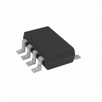
AD5228BUJZ100-R2 Analog Devices Inc, AD5228BUJZ100-R2 Datasheet - Page 14

AD5228BUJZ100-R2
Manufacturer Part Number
AD5228BUJZ100-R2
Description
IC DGTL POT 100K UP/DN TSOT23-8
Manufacturer
Analog Devices Inc
Specifications of AD5228BUJZ100-R2
Temperature Coefficient
35 ppm/°C Typical
Taps
32
Resistance (ohms)
100K
Number Of Circuits
1
Memory Type
Volatile
Interface
Up/Down Counter
Voltage - Supply
2.7 V ~ 5.5 V
Operating Temperature
-40°C ~ 105°C
Mounting Type
Surface Mount
Package / Case
TSOT-23-8, TSOT-8
Resistance In Ohms
100K
End To End Resistance
100kohm
No. Of Steps
32
Resistance Tolerance
± 20%
Supply Voltage Range
2.7V To 5.5V
Control Interface
Pushbutton
No. Of Pots
Single
Lead Free Status / RoHS Status
Lead free / RoHS Compliant
For Use With
EVAL-AD5228EBZ - BOARD EVAL FOR AD5228 DGTL POT
Lead Free Status / RoHS Status
Lead free / RoHS Compliant, Lead free / RoHS Compliant
Available stocks
Company
Part Number
Manufacturer
Quantity
Price
Company:
Part Number:
AD5228BUJZ100-R2
Manufacturer:
AD
Quantity:
15 562
AD5228
POWER-UP AND POWER-DOWN SEQUENCES
Because of the ESD protection diodes that limit the voltage
compliance at Terminals A, B, and W (Figure 39), it is important
to power on V
and W. Otherwise, the diodes are forward-biased such that V
is powered on unintentionally and can affect other parts of the
circuit. Similarly, V
power-on sequence is in the following order: GND, V
V
as long as they are powered on after V
and PD pins can be logic high or floating, but they should not
be logic low during power-on.
A/B/W
. The order of powering V
DD
before applying any voltage to Terminals A, B,
DD
should be powered down last. The ideal
A
, V
B
, and V
DD
. The states of the PU
W
is not important
DD
, and
Rev. 0 | Page 14 of 20
DD
LAYOUT AND POWER SUPPLY BIASING
It is always a good practice to use compact, minimum lead
length layout design. The leads to the input should be as direct
as possible with a minimum conductor length. Ground paths
should have low resistance and low inductance. It is also good
practice to bypass the power supplies with quality capacitors.
Low ESR (equivalent series resistance) 1 µF to 10 µF tantalum
or electrolytic capacitors should be applied at the supplies to
minimize any transient disturbance and to filter low frequency
ripple. Figure 39 illustrates the basic supply bypassing configu-
ration for the AD5228.
V
DD
Figure 40. Power Supply Bypassing
+
C2
10µF
C1
0.1µF
V
AD5228
DD
GND


