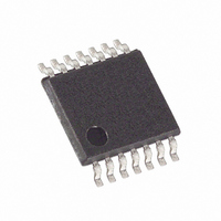
DS1805E-010+ Maxim Integrated Products, DS1805E-010+ Datasheet - Page 9

DS1805E-010+
Manufacturer Part Number
DS1805E-010+
Description
IC POT DIG ADDRESS 10K 14-TSSOP
Manufacturer
Maxim Integrated Products
Datasheet
1.DS1805E-010.pdf
(10 pages)
Specifications of DS1805E-010+
Taps
256
Resistance (ohms)
10K
Number Of Circuits
1
Temperature Coefficient
750 ppm/°C Typical
Memory Type
Volatile
Interface
I²C, 2-Wire Serial
Voltage - Supply
2.7 V ~ 5.5 V
Operating Temperature
-40°C ~ 85°C
Mounting Type
Surface Mount
Package / Case
14-TSSOP
Resistance In Ohms
10K
Lead Free Status / RoHS Status
Lead free / RoHS Compliant
Following the START condition, the DS1805 monitors
the SDA bus checking the device type identifier being
transmitted. Upon receiving the 0101 address code
and appropriate device select bits, the slave device
outputs an acknowledge signal on the SDA line.
The DS1805’s command and protocol structure of the
DS1805 allows the user to read or write to both the
scratchpad and potentiometer registers. Figures 4 and
5 show the command structures for the part.
Potentiometer data values and control and command
values are always transmitted most significant bit
(MSB) first. During communications, the receiving unit
always generates the acknowledge.
As shown in Figure 4, the DS1805 provides one read-
command operation. This operation allows the user to
read both potentiometers. Specifically, the R/W bit of the
control byte is set equal to a one for a read operation.
Communication to read the DS1805 begins with a START
condition that is issued by the master device. The control
byte from the master device follows the START condition.
Once the control byte has been received by the DS1805,
the part responds with an acknowledge. The read/write
bit of the control byte as stated should be set equal to
one for reading the DS1805.
When the master has received the acknowledge from the
DS1805, the master can then begin to receive poten-
tiometer wiper data. The value of the register-0 wiper
position will be the first returned from the DS1805. Once
the eight bits of the register-0 wiper position have been
transmitted, the master needs to issue an acknowledge,
unless it is the only byte to be read, in which case the
master issues a not acknowledge. If desired, the master
can stop the communication transfer at this point by issu-
ing the STOP condition. However, if the value of the
potentiometer-1 wiper position value is needed, commu-
Figure 4. 2-Wire Read Protocols
MSB
0
1
0
Command and Protocol
CONTROL
1
BYTE
A2
A1
Reading the DS1805
A0
Addressable Digital Potentiometer
LSB
1
R/W = 1
_____________________________________________________________________
MSB
REG-0
DATA
BYTE
nication transfer can continue by clocking the remaining
eight bits of the potentiometer-1 value, followed by a not
acknowledge. Final communication transfer is terminated
by issuing the STOP command. Figure 4 shows the flow
of the read operation.
Figure 5 shows a data flow diagram for writing the
DS1805. The DS1805 has three write-command opera-
tions. These include write reg-0, write pot-1, and write
reg-0/pot-1. The write reg-0 command allows the user to
write the value of scratchpad register-0 and as an option
the value of potentiometer-1. The write-1 command allows
the user to write the value of potentiometer-1 only. The
last write command, write-0/1, allows the user to write
both registers to the same value with one command and
one data value being issued.
All the write operations begin with a START condition.
Following the START condition, the master device issues
the control byte. The read/write bit of the control byte is
set to zero for writing the DS1805. Once the control byte
has been issued and the master receives the acknowl-
edgment from the DS1805, the command byte is trans-
mitted to the DS1805. As mentioned above, there exist
three write operations that can be used with the DS1805.
Figure 5 and Table 1 show the binary value of each write
command.
For the latest package outline information, go to
www.maxim-ic.com/packages.
Table 1. 2-Wire Command Words
Write Register-0
Write Potentiometer-1 Register
Write Both Registers
LSB
COMMAND
OPTIONAL
MSB
Package Information
DATA
BYTE
POT-1
Writing to the DS1805
COMMAND VALUE
101010 01
101010 10
101011 11
LSB
9


