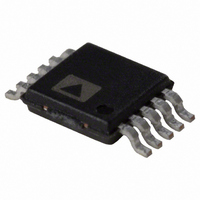
AD5162BRMZ100 Analog Devices Inc, AD5162BRMZ100 Datasheet - Page 16

AD5162BRMZ100
Manufacturer Part Number
AD5162BRMZ100
Description
IC DGTL POT DUAL 100K I2C 10MSOP
Manufacturer
Analog Devices Inc
Datasheet
1.AD5162BRMZ2.5.pdf
(20 pages)
Specifications of AD5162BRMZ100
Temperature Coefficient
35 ppm/°C Typical
Taps
256
Resistance (ohms)
100K
Number Of Circuits
2
Memory Type
Volatile
Interface
SPI, 3-Wire Serial
Voltage - Supply
2.7 V ~ 5.5 V
Operating Temperature
-40°C ~ 125°C
Mounting Type
Surface Mount
Package / Case
10-MSOP, Micro10™, 10-uMAX, 10-uSOP
Resistance In Ohms
100K
End To End Resistance
100kohm
No. Of Steps
256
Resistance Tolerance
± 20%
Supply Voltage Range
2.7V To 5.5V
Control Interface
Serial, 3-Wire
No. Of Pots
Dual
Lead Free Status / RoHS Status
Lead free / RoHS Compliant
For Use With
AD5162EVAL - BOARD EVAL FOR AD5162
Lead Free Status / RoHS Status
Lead free / RoHS Compliant, Lead free / RoHS Compliant
Available stocks
Company
Part Number
Manufacturer
Quantity
Price
Company:
Part Number:
AD5162BRMZ100
Manufacturer:
NXP
Quantity:
2 650
Part Number:
AD5162BRMZ100
Manufacturer:
ADI/亚德诺
Quantity:
20 000
Part Number:
AD5162BRMZ100-RL7
Manufacturer:
ADI/亚德诺
Quantity:
20 000
AD5162
SPI INTERFACE
SPI-COMPATIBLE, 3-WIRE SERIAL BUS
The AD5162 contains a 3-wire, SPI-compatible digital interface
(SDI, CS , and CLK). The 9-bit serial word must be loaded MSB
first. The format of the word is shown in Table 8.
The positive-edge sensitive CLK input requires clean transitions
to avoid clocking incorrect data into the serial input register.
Standard logic families work well. If mechanical switches are
used for product evaluation, they should be debounced by a
flip-flop or another suitable means. When CS is low, the clock
loads data into the serial register on each positive clock edge
(see Figure 42).
The data setup and data hold times in Table 3 determine the
valid timing requirements. The AD5162 uses a 9-bit serial input
data register word that is transferred to the internal RDAC
register when the CS line returns to logic high. Extra MSB bits
are ignored.
(DATA IN)
V
CLK
OUT
SDI
CS
V
DD
1
0
1
0
1
0
0
Figure 43. SPI Interface Detailed Timing Diagram (V
t
CSH0
t
CSS
Dx
t
CH
Rev. C | Page 16 of 20
t
DS
Dx
t
CL
Table 8. Serial Data-Word Format
MSB
B8
A0
(2
1
The values of bits are shown in parentheses.
V
8
CLK
OUT
SDI
)
CS
t
CH
1
0
1
0
1
0
1
0
A
= 5 V, V
B7
D7
(2
t
CSH1
7
)
B
= 0 V, V
A0
Figure 42. SPI Interface Timing Diagram
B6
D6
t
CS1
D7
(V
W
t
S
t
= V
A
CSW
D6
= 5 V, V
B5
D5
OUT
)
D5
B
RDAC REGISTER LOAD
B4
D4
= 0 V, V
±1LSB
D4
D3
1
W
B3
D3
= V
D2
OUT
)
D1
B2
D2
D0
B1
D1
LSB
B0
D0
(2
0
)


