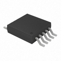
MCP4252-103E/UN Microchip Technology, MCP4252-103E/UN Datasheet - Page 53

MCP4252-103E/UN
Manufacturer Part Number
MCP4252-103E/UN
Description
IC RHEOSTAT 10K 2CH 10MSOP
Manufacturer
Microchip Technology
Datasheet
1.MCP4131-502EP.pdf
(88 pages)
Specifications of MCP4252-103E/UN
Taps
257
Resistance (ohms)
10K
Number Of Circuits
2
Temperature Coefficient
150 ppm/°C Typical
Memory Type
Volatile
Interface
SPI Serial
Voltage - Supply
1.8 V ~ 5.5 V
Operating Temperature
-40°C ~ 125°C
Mounting Type
Surface Mount
Package / Case
10-MSOP, Micro10™, 10-uMAX, 10-uSOP
Resistance In Ohms
10K
End To End Resistance
10kohm
Track Taper
Linear
No. Of Steps
257
Resistance Tolerance
± 20%
Supply Voltage Range
1.8V To 5.5V
Control Interface
Serial, SPI
No. Of Pots
Dual
Lead Free Status / RoHS Status
Lead free / RoHS Compliant
Other names
MCP4252-103-E/UN
MCP4252-103-E/UN
MCP4252-103-E/UN
Available stocks
Company
Part Number
Manufacturer
Quantity
Price
Company:
Part Number:
MCP4252-103E/UN
Manufacturer:
Microchip
Quantity:
367
7.6
The Read command is a 16-bit command. The format
of the command is shown in
The first 6-bits of the Read command determine the
address and the command. The 7th clock will output
the CMDERR bit on the SDO pin. The remaining
9-clocks the device will transmit the 9 data bits (D8:D0)
of the specified address (AD3:AD0).
Figure 7-4
Read command.
FIGURE 7-4:
© 2008 Microchip Technology Inc.
SDI
SDO
Note:
A
D
3
1
1
Read Data
Normal and High Voltage
shows the SDI and SDO information for a
The High Voltage Read Data command is
supported for compatability with system
that also support MCP414X/416X/424X/
426X devices.
D
A
2
1
1
COMMAND BYTE
D
A
1
1
1
D
A
0
1
1
Read Command - SDI and SDO States.
1
1
1
Figure
1
1
1
X
1
0
7-4.
D
X
8
0
D
X
7
0
D
X
6
0
READ DATA
X
D
5
0
MCP413X/415X/423X/425X
DATA BYTE
X
D
4
0
X
D
3
0
X
D
2
0
7.6.1
The read operation requires that the CS pin be in the
active state (V
the inactive state (V
(V
Byte and Data Byte) is then clocked in on the SCK and
SDI pins. The SDO pin starts driving data on the 7th bit
(CMDERR bit) and the addressed data comes out on
the 8th through 16th clocks.
Figure 6-6
Figure 6-5
waveforms when the SDI and SDO signals are
multiplexed on the same pin. For additional information
on the multiplexing of these signals, refer to
Section 6.1.3 “SDI/SDO”.
D
X
1
0
IL
or V
D
X
0
0 Attempted Memory Read of Reserved
IHH
Valid Address/Command combination
Memory location.
show possible waveforms for a single read.
). The 16-bit Read Command (Command
SINGLE READ
and
IL
or V
Figure 6-6
IHH
IH
) and is driven to the active state
). Typically, the CS pin will be in
show the single read
Figure 6-3
DS22060B-page 53
through


