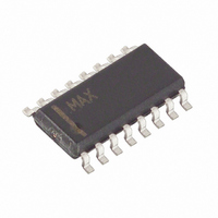
DS1808Z-050+ Maxim Integrated Products, DS1808Z-050+ Datasheet - Page 14

DS1808Z-050+
Manufacturer Part Number
DS1808Z-050+
Description
IC POT DUAL LOG HV 50K 16-SOIC
Manufacturer
Maxim Integrated Products
Datasheet
1.DS1808Z-050.pdf
(17 pages)
Specifications of DS1808Z-050+
Taps
32
Resistance (ohms)
45K
Number Of Circuits
2
Temperature Coefficient
750 ppm/°C Typical
Memory Type
Volatile
Interface
I²C, 2-Wire Serial
Voltage - Supply
4.5 V ~ 5.5 V, ±4.5 V ~ 13.2 V
Operating Temperature
-40°C ~ 85°C
Mounting Type
Surface Mount
Package / Case
16-SOIC (3.9mm Width)
Resistance In Ohms
45K
Number Of Pots
Dual
Taps Per Pot
32
Resistance
45 KOhms
Wiper Memory
Volatile
Digital Interface
Serial (2-Wire)
Operating Supply Voltage
4.5 V to 13.2 V
Supply Current
25 uA
Maximum Operating Temperature
+ 85 C
Minimum Operating Temperature
- 40 C
Description/function
Dual Log Digital Potentiometer
Mounting Style
SMD/SMT
Supply Voltage (max)
13.2 V
Supply Voltage (min)
4.5 V
Tolerance
20 %
Lead Free Status / RoHS Status
Lead free / RoHS Compliant
NOTES
1. All voltages are referenced to ground.
2. I/O pins of fast mode devices must not obstruct the SDA and SCL lines if V
3. The value of V
4. I
5. A fast mode device can be used in a standard mode system, but the requirement t SU:DAT > 250ns
6. After this period, the first clock pulse is generated.
7. The maximum t HD:DAT has only to be met if the device does not stretch the LOW period (t LOW ) of
8. C B – Total capacitance of one bus line in picofarads, timing referenced to (0.9)(V
9. Absolute linearity is used to measure expected wiper voltage as determined by wiper position.
10. Relative linearity is used to determine the change of wiper voltage between two adjacent wiper
11. When used as a rheostat or variable resistor the resistance temperature coefficient is: 750ppm/°C.
12. I
13. Maximum I
either V
levels. Appropriate logic levels specify that logic inputs are within a 0.5V of ground or V
corresponding inactive state.
must then be met. This will automatically be the case if the device does not stretch the LOW period of
the SCL signal. If such a device does stretch the LOW period of the SCL signal, it must output the
next data bit to the SDA line t
released.
the SCL signal.
positions.
When used as a voltage divider or potentiometer, the output voltage temperature coefficient
approaches 30 ppm/°C.
STBY
CC
specified with SDA pin open.
specified for V
:
DD
or V
CC
is dependent on clock rates.
DD
B
. V
should never exceed V
DD
DD
and V
equal to 5.0V. Control port logic pins are driven to the appropriate logic
B
RMAX
can then follow in any order.
+ t SU:DAT = 1000 + 250 = 1250ns before the SCL line is
CC
, including during power-ups. V
14 of 17
CC
CC
must be applied before
is switched off.
DD
) and (0.1)(V
DD
for the
DD
).


