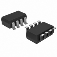
MAX5401EKA+T Maxim Integrated Products, MAX5401EKA+T Datasheet - Page 6

MAX5401EKA+T
Manufacturer Part Number
MAX5401EKA+T
Description
IC DIGITAL POT 256-TAP SOT23-8
Manufacturer
Maxim Integrated Products
Datasheet
1.MAX5400EKAT.pdf
(8 pages)
Specifications of MAX5401EKA+T
Taps
256
Resistance (ohms)
100K
Number Of Circuits
1
Temperature Coefficient
50 ppm/°C Typical
Memory Type
Volatile
Interface
SPI, 3-Wire Serial
Voltage - Supply
2.7 V ~ 5.5 V
Operating Temperature
-40°C ~ 85°C
Mounting Type
Surface Mount
Package / Case
SOT-23-8
Resistance In Ohms
100K
Number Of Pots
Single
Taps Per Pot
256
Resistance
100 KOhms
Wiper Memory
Volatile
Digital Interface
Serial (3-Wire, SPI)
Operating Supply Voltage
5 V
Supply Current
0.0007 mA (Typ)
Maximum Operating Temperature
+ 85 C
Minimum Operating Temperature
- 40 C
Description/function
256-Tap SOT-PoT, Low-Drift Digital Potentiometers in SOT23
Mounting Style
SMD/SMT
Supply Voltage (max)
5.5 V
Supply Voltage (min)
2.7 V
Tolerance
25 %
Lead Free Status / RoHS Status
Lead free / RoHS Compliant
Other names
MAX5401EKA+TTR
The MAX5400/MAX5401 consists of 255 fixed resistors
in series between pins H and L. The potentiometer
wiper (pin W) can be programmed to access any one
of the 256 different tap points on the resistor string. The
MAX5400/MAX5401 uses a 3-wire serial data interface
to control the wiper tap position. This write-only inter-
face contains three inputs: Chip-Select (CS), Data In
(DIN), and Data Clock (SCLK). When CS is taken low,
data from the DIN pin is synchronously loaded into the
8-bit serial shift register on the rising edge of each
SCLK pulse. The MSB is shifted in first as shown in
Figure 4. Note that if CS is not kept low during the entire
data stream, the data will be corrupted and the device
256-Tap SOT-PoT,
Low-Drift Digital Potentiometers in SOT23
Figure 2. Serial Interface Timing Diagram
Figure 3. Detailed Serial Interface Timing Diagram
6
_______________________________________________________________________________________
SCLK
CS
DIN
t
CSO
TIME
SCLK
CS
DIN
Detailed Description
t
CSS
t
DS
MSB
t
DH
D7
1ST CLOCK PULSE
D6
t
CH
D5
t
CL
D4
will need to be reloaded. After all 8 data bits have been
loaded into the shift register, they are latched into the
decoder once CS is taken high. The decoder switches
the potentiometer wiper to the tap position that corre-
sponds to the 8-bit input data. Each resistor cell is
50kΩ/255 or 196.1Ω for the MAX5400 and 100kΩ/255
or 392.2Ω for the MAX5401.
The MAX5400/MAX5401 feature power-on reset (POR)
circuitry that sets the wiper to the midscale position at
power-up by loading a binary value of 128 into the 8-bit
latch.
The MAX5400/MAX5401 can be used as a variable
resistor by connecting pin W to either pin H or pin L.
D3
D2
8TH CLOCK PULSE
t
CP
D1
LSB
D0
POT REGISTER LOADED
t
CSH
t
CS1
t
CSW


