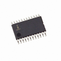
X9252YV24IZ-2.7 Intersil, X9252YV24IZ-2.7 Datasheet - Page 12

X9252YV24IZ-2.7
Manufacturer Part Number
X9252YV24IZ-2.7
Description
IC POT DGTL QUAD 24-TSSOP
Manufacturer
Intersil
Series
XDCP™r
Datasheet
1.X9252YV24IZ-2.7.pdf
(20 pages)
Specifications of X9252YV24IZ-2.7
Taps
256
Resistance (ohms)
2.8K
Number Of Circuits
4
Temperature Coefficient
300 ppm/°C Typical
Memory Type
Non-Volatile
Interface
I²C, 2-Wire Serial
Voltage - Supply
2.7 V ~ 5.5 V
Operating Temperature
-40°C ~ 85°C
Mounting Type
Surface Mount
Package / Case
24-TSSOP
Resistance In Ohms
2.80K
Lead Free Status / RoHS Status
Lead free / RoHS Compliant
Available stocks
Company
Part Number
Manufacturer
Quantity
Price
Company:
Part Number:
X9252YV24IZ-2.7
Manufacturer:
Exar
Quantity:
27
To read or write the contents of a single Data Register or Wiper Register:
1.
2.
RESERVED
FIGURE 6. STATUS REGISTER WRITE (USES STANDARD BYTE WRITE SEQUENCE TO SET UP ACCESS TO A DATA REGISTER)
Load the status register (using a write command) to select the row (See Figure 6)
Writing a 1, 3, 5, or 7 to the Status Register specifies that the subsequent read or write command will access a Data Register. This Status
Register operation also initiates a transfer of the contents of the selected data register to its associated WCR for all DCPs. So, for example,
writing ‘03h’ to the status register causes the value in DR01 to move to WCR0, DR11 to move to WCR1, DR21 to move to WCR2, and DR31
to move to WCR3.
Writing a 0 to bit ‘0’ of the Status Register specifies that the subsequent read or write command will access a Wiper Counter Register. Each
WCR can be written to individually, without affecting the contents of any other.
Access the desired DR or WCR using a new write or read command (see Figure 7 for write and Figure 9 for read.)
Specify the desired column (DCP number) by sending the DCP address as part of this read or write command.
Reserved
BITS 7-3
STATUS REG (Note 1) (Addr: 07H)
Signal at SDA
Signals from
Signals from
DRSel1
the Master
the Slave
bit 2
X
0
0
1
1
12
S
a
t
r
t
0 1 0 1
DRSel0
bit 1
X
0
1
0
1
Address
Slave
TABLE 2. REGISTER NUMBERING
0
NVEnable
A
C
K
bit 0
0 0 0 0 0 1 1 1
0
1
1
1
1
Status Register
Address
X9252
(Addr: 00h)
WCR0
DCP0
DR00
DR01
DR02
DR03
A
C
K
0 0 0 0 0 x x 1
DR select
DR contents move to WCR
REGISTERED SELECTED (Note 2)
Data
If bit 0 of data byte = 1,
during this ACK period
(Addr: 01h)
WCR1
DCP1
DR10
DR12
DR13
DR11
A
C
K
S
o
p
t
(Addr: 02h)
WCR2
DCP2
DR20
DR21
DR22
DR23
(Addr: 03h)
November 14, 2005
WCR3
DCP3
DR30
DR31
DR32
DR33
FN8167.2


