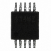
ISL22414WFU10Z Intersil, ISL22414WFU10Z Datasheet - Page 11

ISL22414WFU10Z
Manufacturer Part Number
ISL22414WFU10Z
Description
IC POT DGTL 256TP LN LP 10-MSOP
Manufacturer
Intersil
Series
XDCP™r
Datasheet
1.ISL22414WFU10Z.pdf
(16 pages)
Specifications of ISL22414WFU10Z
Taps
256
Resistance (ohms)
10K
Number Of Circuits
1
Temperature Coefficient
±50ppm/°C
Memory Type
Non-Volatile
Interface
SPI Serial
Voltage - Supply
±2.25 V ~ 5.5 V
Operating Temperature
-40°C ~ 125°C
Mounting Type
Surface Mount
Package / Case
10-MSOP, Micro10™, 10-uMAX, 10-uSOP
Resistance In Ohms
10K
Lead Free Status / RoHS Status
Lead free / RoHS Compliant
Available stocks
Company
Part Number
Manufacturer
Quantity
Price
Company:
Part Number:
ISL22414WFU10Z
Manufacturer:
Intersil
Quantity:
500
Company:
Part Number:
ISL22414WFU10Z-T7A
Manufacturer:
INTERSIL
Quantity:
1 001
is closest to its “Low” terminal (RL). When the WR register of
a DCP contains all ones (WR[7:0]= FFh), its wiper terminal
(RW) is closest to its “High” terminal (RH). As the value of
the WR increases from all zeroes (0) to all ones (255
decimal), the wiper moves monotonically from the position
closest to RL to the closest to RH. At the same time, the
resistance between RW and RL increases monotonically,
while the resistance between RH and RW decreases
monotonically.
While the ISL22414 is being powered up, the WR is reset to
80h (128 decimal), which locates RW roughly at the center
between RL and RH. After the power supply voltage
becomes large enough for reliable non-volatile memory
reading, the WR will be reloaded with the value stored in a
non-volatile Initial Value Register (IVR).
The WR and IVR can be read or written to directly using the
SPI serial interface as described in the following sections.
Memory Description
The ISL22414 contains one non-volatile 8-bit Initial Value
Register (IVR), fourteen non-volatile 8-bit General Purpose
(GP) registers, volatile 8-bit Wiper Register (WR), and
volatile 8-bit Access Control Register (ACR). The memory
map of ISL22414 is in Table 1.
The non-volatile register (IVR) at address 0, contains initial
wiper position and volatile register (WR) contains current
wiper position.
ADDRESS
(hex)
10
E
D
C
B
A
F
9
8
7
6
5
4
3
2
1
0
General Purpose
General Purpose
General Purpose
General Purpose
General Purpose
General Purpose
General Purpose
General Purpose
General Purpose
General Purpose
General Purpose
General Purpose
General Purpose
General Purpose
NON-VOLATILE
TABLE 1. MEMORY MAP
N/A
IVR
11
Reserved
VOLATILE
ACR
N/A
N/A
N/A
N/A
N/A
N/A
N/A
N/A
N/A
N/A
N/A
N/A
N/A
N/A
WR
ISL22414
The register at address 0Fh is a read-only reserved register.
Information read from this register should be ignored.
The non-volatile IVR and volatile WR registers are
accessible with the same address.
The Access Control Register (ACR) contains information
and control bits described below in Table 2.
The VOL bit (ACR[7]) determines whether the access to
wiper registers WR or initial value registers IVR.
If VOL bit is 0, the non-volatile IVR register is accessible. If
VOL bit is 1, only the volatile WR is accessible. Note, value
is written to IVR register also is written to the WR. The
default value of this bit is 0.
The SHDN bit (ACR[6]) disables or enables Shutdown
mode. When this bit is 0, DCP is in Shutdown mode, i.e.
DCP is forced to end-to-end open circuit and RW is shorted
to RL as shown on Figure 15. Default value of SHDN bit is 1.
Setting SHDN bit to 1 is returned wiper to prior to Shutdown
Mode position.
The WIP bit (ACR[5]) is a read-only bit. It indicates that non-
volatile write operation is in progress. The WIP bit can be
read repeatedly after a non-volatile write to determine if the
write has been completed. It is impossible to write or read to
the WR or ACR while WIP bit is 1.
The SDO bit (ACR[1]) configures type of SDO output pin.
The default value of SDO bit is 0 for Push - Pull output. SDO
pin can be configured as Open Drain output for some
application. In this case, an external pull up resistor is
required. See “Applications Information” on page 13.
SPI Serial Interface
The ISL22414 supports an SPI serial protocol, mode 0. The
device is accessed via the SDI input and SDO output with
data clocked in on the rising edge of SCK, and clocked out
on the falling edge of SCK. CS must be LOW during
communication with the ISL22414. SCK and CS lines are
controlled by the host or master. The ISL22414 operates
only as a slave device.
NAME
BIT #
BIT
FIGURE 15. DCP CONNECTION IN SHUTDOWN MODE
TABLE 2. ACCESS CONTROL REGISTER (ACR)
VOL SHDN WIP
7
6
5
4
0
RH
RW
RL
3
0
2
0
December 16, 2010
SDO
1
FN6424.1
0
0


