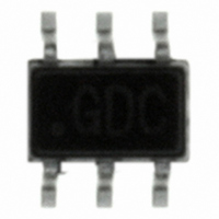
ISL90727WIE627Z-TK Intersil, ISL90727WIE627Z-TK Datasheet - Page 5

ISL90727WIE627Z-TK
Manufacturer Part Number
ISL90727WIE627Z-TK
Description
IC POT DGTL 10K OHM SC70-6
Manufacturer
Intersil
Series
XDCP™r
Datasheet
1.ISL90727WIE627Z-TK.pdf
(8 pages)
Specifications of ISL90727WIE627Z-TK
Taps
128
Resistance (ohms)
10K
Number Of Circuits
1
Temperature Coefficient
45 ppm/°C Typical
Memory Type
Volatile
Interface
I²C, 2-Wire Serial
Voltage - Supply
2.7 V ~ 5.5 V
Operating Temperature
-40°C ~ 85°C
Mounting Type
Surface Mount
Package / Case
SC-70-6, SC-88, SOT-363
Resistance In Ohms
10K
Lead Free Status / RoHS Status
Lead free / RoHS Compliant
Other names
ISL90727WIE627Z-TKTR
Available stocks
Company
Part Number
Manufacturer
Quantity
Price
Company:
Part Number:
ISL90727WIE627Z-TK
Manufacturer:
IDT
Quantity:
2 300
Company:
Part Number:
ISL90727WIE627Z-TK
Manufacturer:
Intersil
Quantity:
8 000
Part Number:
ISL90727WIE627Z-TK
Manufacturer:
INTERSIL
Quantity:
20 000
Operating Specifications
NOTES:
10. R
12. RINL = [R
13.
14. This parameter is not 100% tested.
15. V
16. These are I
17. Parameters with MIN and/or MAX limits are 100% tested at +25°C, unless otherwise specified. Temperature limits established by characterization
11. RDNL = (R
SDA vs SCL Timing
Principles of Operation
The ISL90727 and ISL90728 are integrated circuits
incorporating one DCP with its associated registers and an
I
a host and the potentiometer.
DCP Description
The DCP is implemented with a combination of resistor
elements and CMOS switches. The physical ends of the DCP
are equivalent to the fixed terminals of a mechanical
potentiometer (R
connected to intermediate nodes, and is equivalent to the wiper
terminal of a mechanical potentiometer. The position of the
2
5. Typical values are for T
6. LSB: [V(R
7. ZS error = V(R
8. FS error = [V(R
9. MI =
Rpu (Note 16) SDA and SCL Bus Pull-up Resistor
Cb (Note 16)
C serial interface providing direct communication between
t
F
(OUTPUT TIMING)
SYMBOL
TC
incremental voltage when changing from one tap to an adjacent tap.
R
and are not production tested.
(Note 16)
IL
(INPUT TIMING)
OFFSET
OFFSET
R
= 0V, V
|
=
R
127
--------------------------------------------------------------- -
[
Max Ri
[
W
i
= R
Max Ri
= R
– (MI • i) – R
i
IH
– R
2
)
SDA
SDA
– R
SCL
C-specific parameters and are not directly tested, however, they are used in the device testing to validate specifications.
127
SDA and SCL Fall Time
Capacitive Loading of SDA or SCL
Off-chip
(
= V
127
0
H
W
0
/
(
t
W
MI, when measuring between R
i-1
SU:STA
|
and R
– V(R
)
/
)
)
/
CC.
0
127. R
MI, when measuring between R
127
)
+
) Min Ri
/
/
LSB.
MI - 1, for i = 32 to 127.
–
Min Ri
– V
W
L
A
0
127
)
(
]
pins). The R
PARAMETER
0
= +25°C and 3.3V supply voltage.
CC
/
(
MI, for i = 32 to 127.
]
/
127. V(R
)
and R
]
] 2 ⁄
/
)
t
LSB.
HD:STA
5
]
(Continued)
×
0
-------------------- -
+125°C
are the measured resistances for the DCP register set to FF hex and 00 hex respectively.
W
10
)
W
t
127
6
F
pin of the DCP is
t
SU:DAT
and V(R
for i = 32 to 127, T = -40°C to +85°C. Max( ) is the maximum value of the resistance and Min ( ) is the
minimum value of the resistance over the temperature range.
W
W
and R
W
and R
From 70% to 30% of V
Total on-chip and off-chip
Maximum is determined by t
For Cb = 400pF, max is about 2kΩ ~ 2.5kΩ.
For Cb = 40pF, max is about 15kΩ ~ 20kΩ
)
ISL90727, ISL90728
0
t
HIGH
are V(R
L
.
H
.
W
) for the DCP register set to FF hex and 00 hex respectively. LSB is the
t
TEST CONDITIONS
LOW
t
HD:DAT
wiper terminal within the DCP is controlled by a 7-bit volatile
Wiper Register (WR). The DCP has its own WR. When the WR
of the DCP contains all zeroes (WR<6:0> = 00h), its wiper
terminal (R
WR of the DCP contains all ones (WR<6:0> = 7Fh), its wiper
terminal (R
of the WR increases from all zeroes (00h) to all ones (127
decimal), the wiper moves monotonically from the position
closest to R
the resistance between R
while the resistance between R
monotonically. R
the wiper movement will always be relative to R
CC
R
and t
t
R
W
W
L
F
) is closest to its “Low” terminal (R
) is closest to its “High” terminal (R
to the position closest to R
.
t
AA
L
is connected to the GND pin of the device, so
t
DH
W
(Note 17)
0.1*Cb
and R
20 +
MIN
10
1
H
and R
L
increases monotonically,
t
(Note 5)
BUF
TYP
W
H
. At the same time,
decreases
t
SU:STO
L
(Note 17) UNIT
H
L
). When the
). As the value
.
MAX
250
400
October 10, 2008
FN8247.6
kΩ
pF
ns


