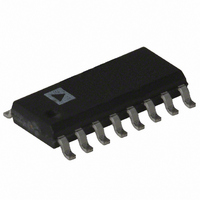
AD5242BRZ100 Analog Devices Inc, AD5242BRZ100 Datasheet - Page 4

AD5242BRZ100
Manufacturer Part Number
AD5242BRZ100
Description
IC POT DGTL DUAL 256POS 16SOIC
Manufacturer
Analog Devices Inc
Datasheet
1.AD5242BRUZ100-RL7.pdf
(20 pages)
Specifications of AD5242BRZ100
Taps
256
Resistance (ohms)
100K
Number Of Circuits
2
Temperature Coefficient
30 ppm/°C Typical
Memory Type
Volatile
Interface
I²C, 2-Wire Serial
Voltage - Supply
2.7 V ~ 5.5 V, ±2.3 V ~ 2.7 V
Operating Temperature
-40°C ~ 105°C
Mounting Type
Surface Mount
Package / Case
16-SOIC (3.9mm Width)
Resistance In Ohms
100K
End To End Resistance
100kohm
No. Of Steps
256
Resistance Tolerance
+50, -30%
Supply Voltage Range
2.7V To 5.5V, ± 2.3V To ± 2.7V
Control Interface
I2C, Serial
No. Of Pots
Dual
Lead Free Status / RoHS Status
Lead free / RoHS Compliant
For Use With
EVAL-AD5242EBZ - BOARD EVALUATION FOR AD5242
Lead Free Status / RoHS Status
Lead free / RoHS Compliant, Lead free / RoHS Compliant
Available stocks
Company
Part Number
Manufacturer
Quantity
Price
Part Number:
AD5242BRZ100
Manufacturer:
AD
Quantity:
20 000
AD5241/AD5242
Parameter
DYNAMIC CHARACTERISTICS
INTERFACE TIMING CHARACTERISTICS
1
2
3
4
5
6
7
8
9
Typicals represent average readings at 25°C, V
Resistor position nonlinearity error R-INL is the deviation from an ideal value measured between the maximum resistance and the minimum resistance wiper
positions. R-DNL measures the relative step change from ideal between successive tap positions. Parts are guaranteed monotonic. See Test Circuits.
INL and DNL are measured at V
specification limits of ±1 LSB maximum are guaranteed monotonic operating conditions. See Figure 37.
Resistor Terminal A, Resistor Terminal B, and Resistor Terminal W have no limitations on polarity with respect to each other.
Guaranteed by design, not subject to production test.
P
Bandwidth, noise, and settling time are dependent on the terminal resistance value chosen. The lowest R value results in the fastest settling time and highest
bandwidth. The highest R value results in the minimum overall power consumption.
All dynamic characteristics use V
See timing diagram in Figure 3 for location of measured values.
DISS
−3 dB Bandwidth
Total Harmonic Distortion
V
Resistor Noise Voltage
(APPLIES TO ALL PARTS
SCL Clock Frequency
Bus Free Time Between Stop and Start, t
Hold Time (Repeated Start), t
Low Period of SCL Clock, t
High Period of SCL Clock, t
Setup Time for Repeated Start Condition, t
Data Hold Time, t
Data Setup Time, t
Rise Time of Both SDA and SCL Signals, t
Fall Time of Both SDA and SCL Signals, t
Setup Time for Stop Condition, t
W
is calculated from (I
Settling Time
HD; DAT
SU; DAT
DD
× V
5, 9
DD
W
). CMOS logic level inputs result in minimum power dissipation.
)
DD
LOW
with the RDAC configured as a potentiometer divider similar to a voltage output D/A converter. V
5, 7, 8
HIGH
= 5 V.
HD; STA
SU; STO
DD
SU; STA
= 5 V.
F
BUF
R
Symbol
BW_10 kΩ
BW_100 kΩ
BW_1 MΩ
THD
t
e
f
t
t
t
t
t
t
t
t
t
t
S
SCL
1
2
3
4
5
6
7
8
9
10
N_WB
W
Rev. C | Page 4 of 20
Conditions
R
R
R
V
V
V
error band, R
R
After this period, the first
clock pulse is generated
AB
AB
AB
A
B
A
WB
= 2 V dc, f = 1 kHz
= 1 V rms + 2 V dc,
= V
= 100 kΩ, code = 0x80
= 10 kΩ, code = 0x80
= 1 MΩ, code = 0x80
= 5 kΩ, f = 1 kHz
DD
, V
B
= 0 V, ± 1 LSB
AB
= 10 kΩ
Min
0
1.3
600
1.3
0.6
600
100
Typ
650
69
6
0.005
2
14
A
= V
1
DD
and V
Max
400
50
900
300
300
B
= 0 V. DNL
Unit
kHz
kHz
kHz
%
μs
nV√Hz
kHz
μs
ns
μs
μs
ns
ns
ns
ns
ns


