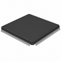
TDA8754HL/27/C1,51 NXP Semiconductors, TDA8754HL/27/C1,51 Datasheet - Page 19

TDA8754HL/27/C1,51
Manufacturer Part Number
TDA8754HL/27/C1,51
Description
IC TRPL 8BIT VIDEO ADC LQFP144
Manufacturer
NXP Semiconductors
Type
Video ADCr
Datasheet
1.TDA8754HL14C155.pdf
(57 pages)
Specifications of TDA8754HL/27/C1,51
Package / Case
144-LQFP
Resolution (bits)
8 b
Sampling Rate (per Second)
270M
Data Interface
Serial
Voltage Supply Source
Analog and Digital
Voltage - Supply
3 V ~ 3.6 V
Operating Temperature
-10°C ~ 70°C
Mounting Type
Surface Mount
Mounting Style
SMD/SMT
Lead Free Status / RoHS Status
Lead free / RoHS Compliant
Other names
935273871518
TDA8754HL27BE-T
TDA8754HL27BE-T
TDA8754HL27BE-T
TDA8754HL27BE-T
Available stocks
Company
Part Number
Manufacturer
Quantity
Price
Company:
Part Number:
TDA8754HL/27/C1,51
Manufacturer:
NXP Semiconductors
Quantity:
10 000
Philips Semiconductors
9397 750 14984
Product data sheet
9.1.2 Write all registers
Table 8:
All registers are programmed one after the other, by giving this initial condition
(XX11 1111) as the subaddress state; thus, the registers are charged following the
predefined sequence of 32 bytes (from subaddress 0 0000 to 1 1111).
Table 9:
Table 10:
Bit
Byte 1
7 to 1
0
Byte 2
7 to 6
5
4 to 0
Byte 3
7 to 0
SDA line Description
S
Byte 1
A
Byte 2
A
Byte 3
A
:
Byte 34
A
P
Byte (2 + n)
Byte 1
Byte 2
Bits
Symbol
A[6:0]
R/W
-
MODE
SA[4:0]
D[7:0]
master starts with a start condition
master transmits device address (7 bits) plus write command bit (R/W = 0)
slave generates an acknowledge
master transmits programming mode and register subaddress to write to
slave generates an acknowledge
master transmits data 1
slave generates an acknowledge
:
master transmits data 32
slave generates an acknowledge
master generates a stop condition
Write format bit description
I
Byte format for writing all registers
2
C-bus sequence for writing all registers
D7
A6
X
7
1
-
programming mode
Rev. 06 — 16 June 2005
Description
Device address; the TDA8754 address is 1001 10X; bit A0 relates
with the voltage level on pin A0
Write command bit; if R/W = 0, then write action
not used
Mode selection bit; if MODE = 0, then each register can be written
independently
Register subaddress; subaddress of the selected register (from
0 0000 to 1 1111)
Data 1; this value is written in the selected register
A5
D6
X
6
0
-
MODE
D5
A4
5
0
0
device address
SA4
D4
A3
4
1
1
data n
Triple 8-bit video ADC up to 270 Msps
SA3
A2
D3
3
1
1
register subaddress
© Koninklijke Philips Electronics N.V. 2005. All rights reserved.
SA2
A1
D2
2
0
1
TDA8754
SA1
D1
A0
X
1
1
R/W
SA0
19 of 57
D0
0
0
1
-


