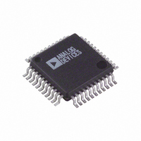
AD7891BS-1 Analog Devices Inc, AD7891BS-1 Datasheet - Page 15

AD7891BS-1
Manufacturer Part Number
AD7891BS-1
Description
IC DAS 12BIT 8CH 44-MQFP
Manufacturer
Analog Devices Inc
Type
Data Acquisition System (DAS)r
Datasheet
1.AD7891BSZ-2.pdf
(20 pages)
Specifications of AD7891BS-1
Rohs Status
RoHS non-compliant
Resolution (bits)
12 b
Sampling Rate (per Second)
500k
Data Interface
Serial, Parallel
Voltage Supply Source
Single Supply
Voltage - Supply
5V
Operating Temperature
-40°C ~ 85°C
Mounting Type
Surface Mount
Package / Case
44-MQFP, 44-PQFP
As in the 8X51 circuit in Figure 7, the way the 68HC11 is
informed that a conversion is completed is not shown in the
diagram. The EOC line can be used to inform the 68HC11
that a conversion is complete by using it as an interrupt signal.
The interrupt service routine reads in the result of the conver-
sion. If a software conversion start is used, the 68HC11 can
wait for 2.0 ms (AD7891-2) or 2.2 ms (AD7891-1) before read-
ing from the AD7891.
AD7891 to ADSP-21xx Serial Interface
An interface between the AD7891 and the ADSP-21xx is shown
in Figure 9. In the interface shown, either SPORT0 or SPORT1
can be used to transfer data to the AD7891. When reading
from the part, the SPORT must be set up with a serial word
length of 16 bits. When writing to the AD7891, a serial word
length of 6 bits or more can be used. Other setups for the
serial interface on the ADSP-21xx internal SCLK use alternate
framing mode and active low framing signal. Normally, the
EOC line from the AD7891 would be connected to the IRQ2
line of the ADSP-21xx to interrupt the DSP at the end of a
conversion (not shown in diagram).
REV. D
Figure 9. AD7891 to ADSP-21xx Serial Interface
*ADDITIONAL PINS OMITTED FOR CLARITY
Figure 8. AD7891 to 68HC11 Interface
*ADDITIONAL PINS OMITTED FOR CLARITY
ADSP-21xx*
68HC11*
MOSO
MOSI
SCLK
SCK
PC6
PC7
RFS
TFS
DT
DR
RFS
TFS
SCLK
DATA IN
DATA OUT
RFS
SCLK
DATA IN
TFS
DATA OUT
AD7891*
AD7891*
–15–
AD7891 to DSP5600x Serial Interface
Figure 10 shows a serial interface between the AD7891 and the
DSP5600x series of DSPs. When reading from the AD7891, the
DSP5600x should be set up for 16-bit data transfers, MSB first,
normal mode synchronous operation, internally generated word
frame sync, and gated clock. When writing to the AD7891, 8-bit
or 16-bit data transfers can be used. The frame sync signal from
the DSP5600x must be inverted before being applied to the
RFS and TFS inputs of the AD7891, as shown in Figure 10.
To monitor the conversion time of the AD7891, a scheme such
as those outlined in previous interfaces with EOC can be used.
This can be implemented by connecting the EOC line directly
to the IRQA input of the DSP5600x.
AD7891 to TMS320xxx Serial Interface
The AD7891 can be interfaced to the serial port of TMS320xxx
DSPs, as shown in Figure 11. External timing generation circuitry
is necessary to generate the serial clock and syncs necessary for
the interface.
Figure 11. AD7891 to TMS320xxx Serial Interface
Figure 10. AD7891 to DSP5600x Serial Interface
TMS320xxx*
*ADDITIONAL PINS OMITTED FOR CLARITY
*ADDITIONAL PINS OMITTED FOR CLARITY
DSP5600x*
FST (SC2)
CLKR
CLKX
SCK
STD
SRD
FSR
FSX
DX
DR
GENERATION
CIRCUITRY
TIMING
SCLK
DATA IN
SCLK
DATA IN
RFS
TFS
DATA OUT
RFS
TFS
DATA OUT
AD7891*
AD7891*
AD7891


