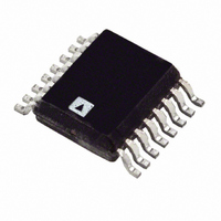
AD7873BRQ Analog Devices Inc, AD7873BRQ Datasheet - Page 21

AD7873BRQ
Manufacturer Part Number
AD7873BRQ
Description
IC ADC 12BIT TOUCHSCREEN 16-QSOP
Manufacturer
Analog Devices Inc
Type
Resistiver
Datasheet
1.AD7873ACPZ-REEL.pdf
(28 pages)
Specifications of AD7873BRQ
Rohs Status
RoHS non-compliant
Touch Panel Interface
4-Wire
Number Of Inputs/keys
1 TSC
Resolution (bits)
12 b
Data Interface
Serial
Data Rate/sampling Rate (sps, Bps)
125k
Voltage Reference
External, Internal
Voltage - Supply
2.2 V ~ 5.25 V
Operating Temperature
-40°C ~ 85°C
Mounting Type
Surface Mount
Package / Case
16-QSOP
Voltage Supply Source
Single Supply
Sampling Rate (per Second)
125k
Lead Free Status / RoHS Status
Not Compliant
Available stocks
Company
Part Number
Manufacturer
Quantity
Price
Part Number:
AD7873BRQZ
Manufacturer:
ADI/亚德诺
Quantity:
20 000
SERIAL INTERFACE
Figure 36 shows the typical operation of the serial interface of
the AD7873. The serial clock provides the conversion clock and
also controls the transfer of information to and from the AD7873.
One complete conversion can be achieved with 24 DCLK cycles.
The CS signal initiates the data transfer and conversion process.
The falling edge of CS takes the BUSY output and the serial bus
out of three-state. The first eight DCLK cycles are used to write
to the control register via the DIN pin. The control register is
updated in stages as each bit is clocked in. Once the converter
has enough information about the following conversion to set
the input multiplexer and switches appropriately, the converter
enters the acquisition mode and, if required, the internal switches
are turned on. During acquisition mode, the reference input
data is updated. After the three DCLK cycles of acquisition, the
control word is complete (the power management bits are now
X/Y SWITCHES
(SER/DFR HIGH)
(SER/DFR LOW)
X/Y SWITCHES
DOUT
DCLK
BUSY
NOTES
1
2
DIN
CS
Y DRIVERS ARE ON WHEN X+ IS SELECTED INPUT CHANNEL (A2 TO A0 = 001); X DRIVERS ARE ON WHEN Y+ IS SELECTED INPUT CHANNEL (A2 TO A0 = 101).
WHEN PD1, PD0 = 00, 01 OR 10, Y– WILL TURN ON AT THE END OF THE CONVERSION.
DRIVERS WILL REMAIN ON IF POWER-DOWN MODE IS 11 (NO POWER-DOWN) UNTIL SELECTED INPUT CHANNEL, REFERENCE MODE,
OR POWER-DOWN MODE IS CHANGED, OR CS IS HIGH.
1, 2
Figure 36. Conversion Timing, 24 DCLKS per Conversion Cycle, 8-Bit Bus Interface. No DCLK delay required with dedicated serial port.
1
THREE-STATE
THREE-STATE
(START)
DCLK
BUSY
DOUT
S
DIN
OFF
OFF
CS
1
A2
A1
IDLE
t
1
A0
t
t
2
3
MODE
t
7
SER/
DFR
ON
t
ACQUIRE
t
8
4
t
PD1 PD0
ACQ
t
5
8
Figure 37. Detail Timing Diagram
PD0
(MSB)
1
Rev. E | Page 21 of 28
11
t
6
10
ON
t
6
9
updated) and the converter enters conversion mode. At this
point, track-and-hold goes into hold mode, the input signal is
sampled, and the BUSY output goes high (BUSY returns low on
the next falling edge of DCLK). The internal switches can also
turn off at this point if in single-ended mode, battery-monitor
mode, or temperature measurement mode.
The next 12 DCLK cycles are used to perform the conversion
and to clock out the conversion result. If the conversion is
ratiometric (SER/ DFR low), the internal switches are on during
the conversion. A 13th DCLK cycle is needed to allow the
DSP/micro to clock in the LSB. Three more DCLK cycles clock
out the three trailing zeros and complete the 24 DCLK transfer.
The 24 DCLK cycles can be provided from a DSP or via three
bursts of eight clock cycles from a microcontroller.
DB11
CONVERSION
8
t
OFF
9
7
DB10
6
8
5
4
1
3
t
t
11
12
2
t
10
1
(LSB)
0
IDLE
ZERO FILLED
OFF
THREE-STATE
THREE-STATE
8
AD7873


