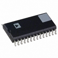
AD7729AR Analog Devices Inc, AD7729AR Datasheet - Page 7

AD7729AR
Manufacturer Part Number
AD7729AR
Description
IC ADC 15BIT DUAL W/DAC 28-SOIC
Manufacturer
Analog Devices Inc
Type
ADC, DACr
Datasheet
1.AD7729ARUZ-REEL.pdf
(16 pages)
Specifications of AD7729AR
Rohs Status
RoHS non-compliant
Resolution (bits)
15 b
Sampling Rate (per Second)
270.8k
Data Interface
Serial
Voltage Supply Source
Analog and Digital
Voltage - Supply
3V
Operating Temperature
-40°C ~ 105°C
Mounting Type
Surface Mount
Package / Case
28-SOIC (7.5mm Width)
Available stocks
Company
Part Number
Manufacturer
Quantity
Price
Company:
Part Number:
AD7729ARU
Manufacturer:
LT
Quantity:
5 460
Part Number:
AD7729ARU
Manufacturer:
ADI/亚德诺
Quantity:
20 000
Company:
Part Number:
AD7729ARUREEL
Manufacturer:
AD
Quantity:
7 066
Part Number:
AD7729ARUZ
Manufacturer:
ADI/亚德诺
Quantity:
20 000
Company:
Part Number:
AD7729ARUZREEL7
Manufacturer:
VISHAY
Quantity:
2 776
Part Number:
AD7729ARZ
Manufacturer:
ADI/亚德诺
Quantity:
20 000
Company:
Part Number:
AD7729ARZ-RL
Manufacturer:
NXP
Quantity:
36 000
Pin
Number
15
13
Power Supply
6
5
7
25
24
23
Analog Signal and Reference
1, 2
3, 4
26
28
27
Auxiliary Serial Port (ASPORT)
10
9
8
20
21
22
Baseband Serial Port (BSPORT)
16
12
11
17
18
19
ADCs
14
REV. 0
Mnemonic
MCLK
RESETB
AVDD1
AVDD2
AGND
DVDD1
DVDD2
DGND
IRxP, IRxN
QRxP, QRxN
AUXDAC
REFCAP
REFOUT
ASCLK
ASDI
ASDIFS
ASDO
ASDOFS
ASE
BSCLK
BSDI
BSDIFS
BSDO
BSDOFS
BSE
RxON
Function
Master Clock Input. MCLK is driven from a 13 MHz crystal. The active levels for MCLK are
determined by the value of DVDD2.
Active Low Reset Signal. This input resets the entire AD7729 chip, resetting the control
registers and clearing the digital filters. The logic input levels (V
are determined by the value of DVDD2.
Analog Power Supply Connection for the Rx Section and the Bandgap Reference.
Analog Power Supply Connection for the Auxiliary Section.
Analog Ground Connection.
Digital Power Supply Connection.
Digital Power Supply Connection for the Serial Interface Section. This power supply also sets
the threshold voltages for RxON, RESETB and MCLK.
Digital Ground Connection.
Differential Analog Input for I Receive Channel.
Differential Analog Input for Q Receive Channel.
Analog Output Voltage from the 10-Bit Auxiliary DAC AUXDAC. This DAC is used for
functions such as Automatic Gain Control (AGC). The DAC possesses a register that is
accessible via the ASPORT or BSPORT. The DAC may be individually powered down.
A bypass capacitor to AGND of 0.1 F is required for the on-chip reference. The capacitor
should be fixed to this pin.
Buffered Reference Output, which has a nominal value of 1.3 V. A bypass capacitor (to
AGND) of 0.1 F is required on this pin.
Serial Clock used to clock data or control bits to and from the auxiliary serial port (ASPORT).
The frequency of ASCLK is programmable and is equal to the frequency of the master clock
(MCLK) divided by an integer number.
Serial Data Input of ASPORT. Both data and control information are input on this pin.
Input Framing Signal for ASDI Serial Transfers.
Serial Data Output of ASPORT. Both data and control information are output on this pin.
ASDO is in three-state when no information is being transmitted, thereby allowing external
control.
Output Framing Signal for ASDO Serial Transfers.
ASPORT Enable. When ASE is low, the ASPORT is put into three-state thereby allowing
external control of the serial bus.
Output serial clock used to clock data or control bits to and from the baseband serial port
(BSPORT). The frequency of BSCLK is programmable and is equal to the frequency of the
master clock (MCLK) divided by an integer number.
Serial Data Input of BSPORT. Both data and control information are input on this pin.
Input Framing Signal for BSDI Serial Transfers.
Serial Data Output of BSPORT. Both data and control information are output on this pin.
BSDO is in three-state when no information is being transmitted, thereby allowing external
control.
Output Framing Signal for BSDO Serial Transfers.
BSPORT Enable. When BSE is low, the BSPORT is put into three-state thereby allowing
external control of the serial bus.
Receive Section Power-On Digital Input. The receive section is powered up by taking pin
RxON high. The receive section can alternatively be powered up by programming bit RxON
in baseband control register BCRA. When the powering up/down of the receive section is
being controlled by pin RxON, bit RxON should equal zero. Similarly, when the powering up/
down of the receive section is being controlled by bit RxON, pin RxON should be tied low.
The logic input levels (V
PIN FUNCTION DESCRIPTIONS
INH
–7–
and V
INL
) for RxON are determined by the value of DVDD2.
INH
and V
INL
) for RESETB
AD7729


