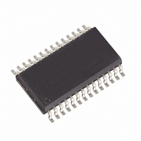
MAX199BEWI+ Maxim Integrated Products, MAX199BEWI+ Datasheet - Page 8

MAX199BEWI+
Manufacturer Part Number
MAX199BEWI+
Description
IC DAS 12BIT 8CH 28-SOIC
Manufacturer
Maxim Integrated Products
Type
Data Acquisition System (DAS)r
Datasheet
1.MAX199BCWI.pdf
(16 pages)
Specifications of MAX199BEWI+
Resolution (bits)
12 b
Sampling Rate (per Second)
100k
Data Interface
Parallel
Voltage Supply Source
Single Supply
Voltage - Supply
4.75 V ~ 5.25 V
Operating Temperature
-40°C ~ 85°C
Mounting Type
Surface Mount
Package / Case
28-SOIC (7.5mm Width)
Lead Free Status / RoHS Status
Lead free / RoHS Compliant
The MAX199, a multi-range, fault-tolerant ADC, uses
successive approximation and internal input track/hold
(T/H) circuitry to convert an analog signal to a 12-bit
digital output. The parallel-output format provides easy
interface to microprocessors (µPs). Figure 3 shows the
MAX199 in its simplest operational configuration.
In the internal acquisition control mode (control bit D5
set to 0), the T/H enters its tracking mode on WR’s ris-
ing edge, and enters its hold mode when the internally
timed (6 clock cycles) acquisition interval ends. In bipo-
lar mode, a low-impedance input source, which settles
in less than 1.5µs, is required to maintain conversion
accuracy at the maximum conversion rate.
When configured for unipolar mode, the input does not
need to be driven from a low-impedance source. The
acquisition time (t
resistance (R
the T/H capacitance.
Acquisition time is calculated by:
Multi-Range (±4V, ±2V, +4V, +2V),
+5V Supply, 12-Bit DAS with 8+4 Bus Interface
Figure 3. Operational Diagram
8
_______________Detailed Description
CONTROL
INPUTS
_______________________________________________________________________________________
P
For 0V to V
For 0V to V
P DATA BUS
S
), the channel input resistance (R
100pF
REF
REF/2
10
11
12
13
14
1
2
3
4
5
6
7
8
9
AZ
: t
WR
RD
D6
D1/D9
CLK
CS
HBEN
SHDN
D7
D5
D4
D3/D11
D2/D10
D0/D8
) is a function of the source output
: t
AZ
AZ
MAX199
= 9 x (R
Analog-Input Track/Hold
= 9 x (R
Converter Operation
REFADJ
DGND
AGND
CH7
CH6
CH5
CH4
CH3
CH2
CH1
CH0
V
REF
INT
S
DD
S
+ R
+ R
28
27
26
25
24
23
22
21
20
19
18
17
16
15
IN
IN
) x 16pF
0.1 F
) x 32pF
OUTPUT STATUS
ANALOG
INPUTS
IN
), and
+4.096V
4.7 F
+5V
where R
V
In the external acquisition control mode (D5 = 1), the
T/H enters its tracking mode on the first WR rising edge
and enters its hold mode when it detects the second WR
rising edge with D5 = 0. See the External Acquisition
section.
The ADC’s input tracking circuitry has a 5MHz small-
signal bandwidth. When using the internal acquisition
mode with an external clock frequency of 2MHz, a
100ksps throughput rate can be achieved. It is possible
to digitize high-speed transient events and measure
periodic signals with bandwidths exceeding the ADC’s
sampling rate by using undersampling techniques. To
avoid high-frequency signals being aliased into the fre-
quency band of interest, anti-alias filtering is recom-
mended (MAX274/MAX275 continuous-time filters).
Figure 4 shows the equivalent input circuit. The MAX199
can be programmed for input ranges of ±V
0V to V
control bits (D3, D4) in the control byte (see Tables 1 and
2). When an external reference is applied at REFADJ, the
voltage at REF is given by V
< V
Figure 4. Equivalent Input Circuit
REF
S1 = BIPOLAR/UNIPOLAR SWITCH
S2 = INPUT MUX SWITCH
S3, S4 = T/H SWITCH
CH_
REF
range) or 3µs (0V to V
< 4.18V).
5.12k
REF
IN
= 7kΩ, and t
, or 0V to V
5.12k
S1
S2
Input Range and Protection
HOLD
REF/2
AZ
UNIPOLAR
BIPOLAR
OFF
ON
is never less than 2µs (0V to
REF
REF/2
by setting the appropriate
S3
= 1.6384 x V
TRACK
range).
Input Bandwidth
C
HOLD
TRACK
REF
S4
REFADJ
VOLTAGE
REFERENCE
, ±V
T/H
OUT
REF/2
HOLD
(2.4V
,


