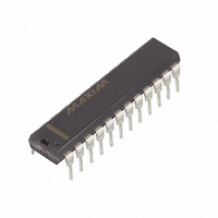
MAX1271ACNG+ Maxim Integrated Products, MAX1271ACNG+ Datasheet - Page 9

MAX1271ACNG+
Manufacturer Part Number
MAX1271ACNG+
Description
IC ADC 12BIT 8CH 24-DIP
Manufacturer
Maxim Integrated Products
Type
Data Acquisition System (DAS)r
Datasheet
1.MAX1270BCAI.pdf
(20 pages)
Specifications of MAX1271ACNG+
Resolution (bits)
12 b
Sampling Rate (per Second)
110k
Data Interface
Serial
Voltage Supply Source
Single Supply
Voltage - Supply
4.75 V ~ 5.25 V
Operating Temperature
0°C ~ 70°C
Mounting Type
Through Hole
Package / Case
24-DIP (0.300", 7.62mm)
Lead Free Status / RoHS Status
Lead free / RoHS Compliant
The MAX1270/MAX1271 multirange, fault-tolerant ADCs
use successive approximation and internal track/hold
(T/H) circuitry to convert an analog signal to a 12-bit
digital output. Figure 3 shows the block diagram of the
MAX1270/MAX1271.
The T/H enters tracking/acquisition mode on the falling
edge of the sixth clock in the 8-bit input control word,
and enters hold/conversion mode when the timed
acquisition interval (six clock cycles, 3µs minimum)
ends. In internal clock mode, the acquisition is timed by
two external clock cycles and four internal clock cycles.
Figure 1. Reference-Adjust Circuit
Figure 3. Block Diagram
REFADJ
100kΩ
24kΩ
SHDN
CH0
CH1
CH2
CH3
CH4
CH5
CH6
CH7
REF
+5V
510kΩ
_______________________________________________________________________________________
0.01µF
REFERENCE
CONDITIONING
Detailed Description
AND SIGNAL
2.5V
Analog-Input Track/Hold
ANALOG
INPUT
MUX
Converter Operation
REFADJ
10kΩ
MAX1270
MAX1271
1.638
Av =
Multirange, +5V, 8-Channel,
DIN
SERIAL INTERFACE LOGIC
T/H
+4.096V
SSTRB
When operating in bipolar (MAX1270 and MAX1271) or
unipolar mode (MAX1270) the signal applied at the
input channel is rescaled through the resistor-divider
network formed by R1, R2, and R3 (Figure 4); a low
impedance (<4Ω) input source is recommended to
minimize gain error. When the MAX1271 is configured
for unipolar mode, the channel input resistance (R
becomes a fixed 5.12kΩ (typ). Source impedances
below 15kΩ (0 to V
significantly affect the AC performance of the ADC.
The acquisition time (t
output resistance, the channel input resistance, and the
T/H capacitance. Higher source impedances can be
used if an input capacitor is connected between the
analog inputs and AGND. Note that the input capacitor
forms an RC filter with the input source impedance, lim-
iting the ADC’s signal bandwidth.
Figure 2. Output Load Circuit for Timing Characteristics
SSTRB
DOUT
OR
a) HIGH IMPEDANCE TO V
0.5mA
DOUT
V
OH
AND V
Serial 12-Bit ADCs
CS
IN
REF
OH
OUT
TO HIGH IMPEDANCE
12-BIT SAR ADC
OH
MAX1270
MAX1271
REF
C
LOAD
, V
ACQ
OL
) and 5kΩ (0 to V
TO
) is a function of the source
SCLK
CLOCK
b)
SSTRB
DOUT
HIGH IMPEDANCE TO V
V
OH
OR
CLOCK
INT
AND V
5mA
OH
+5V
TO HIGH IMPEDANCE
REF
C
LOAD
/2) do not
OH
, V
V
AGND
DGND
OL
DD
TO
IN
9
)


