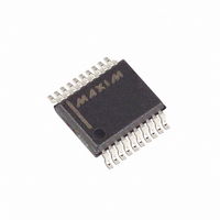
MAX192BCAP+ Maxim Integrated Products, MAX192BCAP+ Datasheet - Page 2

MAX192BCAP+
Manufacturer Part Number
MAX192BCAP+
Description
IC ADC LP 10-BIT 133KHZ 20-SSOP
Manufacturer
Maxim Integrated Products
Type
Data Acquisition System (DAS), ADCr
Datasheet
1.MAX192BEWP.pdf
(24 pages)
Specifications of MAX192BCAP+
Resolution (bits)
10 b
Sampling Rate (per Second)
133k
Data Interface
Serial
Voltage Supply Source
Single Supply
Voltage - Supply
±5V
Operating Temperature
0°C ~ 70°C
Mounting Type
Surface Mount
Package / Case
20-SSOP
Lead Free Status / RoHS Status
Lead free / RoHS Compliant
V
AGND to DGND.................................................... -0.3V to +0.3V
CH0–CH7 to AGND, DGND ...................... -0.3V to (V
CH0–CH7 Total Input Current.......................................... ±20mA
VREF to AGND .......................................... -0.3V to (V
REFADJ to AGND...................................... -0.3V to (V
Digital Inputs to DGND.............................. -0.3V to (V
Digital Outputs to DGND ........................... -0.3V to (V
Digital Output Sink Current .................................................25mA
ELECTRICAL CHARACTERISTICS
(V
T
Low-Power, 8-Channel,
Serial 10-Bit ADC
Stresses beyond those listed under “Absolute Maximum Ratings” may cause permanent damage to the device. These are stress ratings only, and functional
operation of the device at these or any other conditions beyond those indicated in the operational sections of the specifications is not implied. Exposure to
absolute maximum rating conditions for extended periods may affect device reliability.
2
ABSOLUTE MAXIMUM RATINGS
A
DD
DC ACCURACY (Note 1)
DYNAMIC SPECIFICATIONS (10kHz sine-wave input, 4.096Vp-p, 133ksps, 2.0MHz external clock)
CONVERSION RATE
Resolution
Relative Accuracy (Note 2)
Differential Nonlinearity
Offset Error
Gain Error
Gain Temperature Coefficient
Channel-to-Channel
Offset Matching
Signal-to-Noise + Distortion Ratio
Total Harmonic Distortion
(up to the 5th harmonic)
Spurious-Free Dynamic Range
Channel-to-Channel Crosstalk
Small-Signal Bandwidth
Full-Power Bandwidth
Conversion Time (Note 4)
Track/Hold Acquisition Time
Aperture Delay
Aperture Jitter
Internal Clock Frequency
DD
= T
_______________________________________________________________________________________
to AGND........................................................... -0.3V to +6V
= 5V ±5%, f
MIN
PARAMETER
to T
MAX,
CLK
unless otherwise noted. Typical values are at T
= 2.0MHz, external clock (50% duty cycle), 15 clocks/conversion cycle (133ksps), 4.7µF capacitor at VREF pin,
SYMBOL
SINAD
t
SFDR
CONV
DNL
THD
t
AZ
MAX192A
MAX192B
No missing codes over temperature
External reference, 4.096V
External reference, 4.096V
65kHz, V
-3dB rolloff
Internal clock
External clock, 2MHz, 12 clocks/conversion
DD
DD
DD
DD
DD
+ 0.3V)
+ 0.3V)
+ 0.3V)
+ 0.3V)
+ 0.3V)
IN
= 4.096Vp-p (Note 3)
CONDITIONS
A
= +25°C.)
Continuous Power Dissipation (T
Operating Temperature Ranges
Storage Temperature Range ............................ -60°C to +150°C
Lead Temperature (soldering, 10sec) ............................ +300°C
Plastic DIP (derate 11.11mW/°C above +70°C) ......... 889mW
SO (derate 10.00mW/°C above +70°C) ...................... 800mW
SSOP (derate 8.00mW/°C above +70°C) ................... 640mW
CERDIP (derate 11.11mW/°C above +70°C) .............. 889mW
MAX192_C_P ..................................................... 0°C to +70°C
MAX192_E_P .................................................. -40°C to +85°C
MAX192_MJP ............................................... -55°C to +125°C
MIN
5.5
10
6
A
= +70°C)
±0.8
±0.1
TYP
800
<50
-70
-75
4.5
1.7
66
70
10
MAX
±1/2
1.5
±1
±1
±2
±2
10
ppm/°C
UNITS
MHz
MHz
LSB
LSB
LSB
LSB
LSB
Bits
kHz
dB
dB
dB
dB
µs
µs
ns
ps


