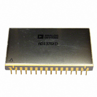
AD2S44-TM18B Analog Devices Inc, AD2S44-TM18B Datasheet - Page 7

AD2S44-TM18B
Manufacturer Part Number
AD2S44-TM18B
Description
IC CONV SYNC/R-D 14BIT 2CH 32DIP
Manufacturer
Analog Devices Inc
Type
R/D Converterr
Datasheet
1.AD2S44-TM11B.pdf
(12 pages)
Specifications of AD2S44-TM18B
Resolution (bits)
14 b
Data Interface
Parallel
Voltage Supply Source
Dual ±
Voltage - Supply
±14.25 V ~ 15 V
Operating Temperature
-55°C ~ 125°C
Mounting Type
Through Hole
Package / Case
32-CDIP (0.900", 22.86mm)
Lead Free Status / RoHS Status
Lead free / RoHS Compliant
Sampling Rate (per Second)
-
Other names
AD2S44TM18B
AD2S44TM18B
AD2S44TM18B
Available stocks
Company
Part Number
Manufacturer
Quantity
Price
Company:
Part Number:
AD2S44-TM18B
Manufacturer:
HITTITE
Quantity:
124
THEORY OF OPERATION
The AD2S44 operates on a tracking principle. The output digital
word continually tracks the position of the synchro/resolver shaft
without the need for external convert commands and status wait
loops. As the transducer moves through a position equivalent
to the least significant bit weighting, the output digital word is
updated.
Each channel is identical in operation, sharing power supply and
output pins. Both channels operate continuously and indepen-
dently of each other. The digital output from either channel is
available after switching the channel select and output enable
inputs.
If the device is a synchro-to-digital converter, the 3-wire synchro
output is connected to the S1, S2, and S3 pins on the unit, and
a solid-state Scott T input conditioner converts these signals into
resolver format given by
where:
θ is the angle of the synchro shaft.
E
K is the transformation ratio of the input signal conditioner.
If the unit is a resolver-to-digital converter, the 4-wire resolver
output is connected directly to the S1, S2, S3, and S4 pins on
the unit.
To understand the conversion process, assume that the current
word state of the up-down counter is ϕ. V
and V
These signals are subtracted by the error amplifier to give
0
sin ωt is the reference signal.
V
V
K E
K E
K E
or
K E
2
1
2
is multiplied by sin ϕ to give the following:
= K E
= K E
0
0
0
0
sin ωt sin θ cos ϕ
sin ωt cos θ sin ϕ
sin ωt (sin θ cos ϕ − cos θ sin ϕ)
sin ωt sin (θ − ϕ)
0
0
sin ωt sin θ
sin ωt cos θ
R
R
R
R
S1 (A)
S2 (A)
S3 (A)
S4 (A)
S1 (B)
S2 (B)
S3 (B)
S4 (B)
LO
LO
HI
HI
(A)
(A)
(B)
(B)
CONDITIONER
CONDITIONER
CONDITIONER
CONDITIONER
REFERENCE
REFERENCE
RESOLVER
RESOLVER
SYNCHRO/
SYNCHRO/
AD2S44
1
is multiplied by cos ϕ,
V
V
1
2
MULTIPLIER
MULTIPLIER
SIN/COS
SIN/COS
SPEED
SPEED
HIGH
HIGH
Figure 3. Functional Block Diagram
ERROR
ERROR
AMP
AMP
DETECTION
BUILT-IN
TEST
Rev. A | Page 7 of 12
DETECTOR
DETECTOR
SENSITIVE
SENSITIVE
PHASE-
PHASE-
A phase sensitive detector, integrator, and voltage-controlled
oscillator (VCO) form a closed-loop system that seeks to null sin
(θ − ϕ). When this is accomplished, the word state of the up-down
counter (ϕ) equals the synchro/resolver shaft angle (θ), to within
the rated accuracy of the converter.
CONNECTING THE CONVERTER
The power supply voltages connected to −V
±15 V and cannot be reversed.
It is suggested that a parallel combination of a ceramic 100 nF
capacitor and a tantalum 6.8 μF capacitor be placed from each
of the supply pins to GND.
The pin marked GND is connected electrically to the case and
is to be taken to 0 V potential in the system.
The digital output is taken from Pin 26 to Pin 32 and from Pin 1
to Pin 7. Pin 26 is the MSB, and Pin 7 is the LSB.
The reference connections are made to the R
pins. In the case of a synchro, the signals are connected to the
S1, S2, and S3 pins, according to the following convention:
For a resolver, the signals are connected to the S1, S2, S3, and S4
pins, according to the following convention:
CHANNEL SELECT (A/B)
A/ B is the channel select input. A Logic 1 selects Channel A, and
a Logic 0 selects Channel B. Data becomes valid 640 ns after A/ B
is toggled. Timing information is shown in
INTEGRATOR
INTEGRATOR
E
E
E
E
E
S1−S3
S3−S2
S2−S1
S1−S3
S2−S4
= E
= E
= E
= E
= E
RLO−RHI
RLO−RHI
RLO−RHI
RLO−RHI
RLO−RHI
VCO
VCO
sin ωt sin θ
sin ωt sin (θ − 120°)
sin ωt sin (θ – 240°)
sin ωt sin θ
sin ωt cos θ
COUNTER
COUNTER
UP-DOWN
LATCHES
UP-DOWN
OUTPUT
THREE-
STATE
A/B
OE
DB1 (LSB)
TO
DB14 (MSB)
+V
GND
–V
BIT
S
S
Figure 4
S
HI
and +V
pins and the R
and
AD2S44
S
are to be
Figure 5
LO
.


