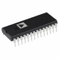
AD7874ANZ Analog Devices Inc, AD7874ANZ Datasheet - Page 2

AD7874ANZ
Manufacturer Part Number
AD7874ANZ
Description
IC DAS 12BIT 4CH LC2MOS 28-DIP
Manufacturer
Analog Devices Inc
Type
Data Acquisition System (DAS)r
Datasheet
1.AD7874ARZ.pdf
(16 pages)
Specifications of AD7874ANZ
Resolution (bits)
12 b
Data Interface
Parallel
Sampling Rate (per Second)
116k
Voltage Supply Source
Dual ±
Voltage - Supply
5V
Operating Temperature
-40°C ~ 85°C
Mounting Type
Through Hole
Package / Case
28-DIP (0.600", 15.24mm)
Sampling Rate
116kSPS
Input Channel Type
Single Ended
Supply Voltage Range - Analog
± 4.75V To ± 5.25V
Supply Current
12mA
Lead Free Status / RoHS Status
Lead free / RoHS Compliant
Available stocks
Company
Part Number
Manufacturer
Quantity
Price
Company:
Part Number:
AD7874ANZ
Manufacturer:
AD
Quantity:
5 530
Parameter
SAMPLE-AND-HOLD
SAMPLE-AND-HOLD AND ADC
DC ACCURACY
ANALOG INPUTS
REFERENCE OUTPUTS
REFERENCE INPUT
LOGIC INPUTS
LOGIC OUTPUTS
POWER REQUIREMENTS
NOTES
1
2
3
4
5
Specifications subject to change without notice.
AD7874–SPECIFICATIONS
Temperature ranges are as follows: A, B Versions: –40 C to +85 C; S Version: –55 C to +125 C.
See Terminology.
Sample tested @ +25 C to ensure compliance.
Measured with respect to the REF IN voltage and includes bipolar offset error.
For capacitive loads greater than 50 pF a series resistor is required.
Acquisition Time
Droop Rate
–3 dB Small Signal Bandwidth
Aperture Delay
Aperture Jitter
Aperture Delay Matching
DYNAMIC PERFORMANCE
Signal-to-Noise Ratio
Total Harmonic Distortion
Peak Harmonic or Spurious Noise
Intermodulation Distortion
Channel-to-Channel Isolation
Resolution
Relative Accuracy
Differential Nonlinearity
Positive Full-Scale Error
Negative Full-Scale Error
Full-Scale Error Match
Bipolar Zero Error
Bipolar Zero Error Match
Input Voltage Range
Input Current
REF OUT
REF OUT Error @ +25 C
REF OUT Temperature Coefficient
Reference Load Change
Input Voltage Range
Input Current
Input Capacitance
Input High Voltage, V
Input Low Voltage, V
Input Current, I
Input Capacitance, C
Output High Voltage, V
Output Low Voltage, V
DB0–DB11
V
V
I
I
Power Dissipation
DD
SS
DD
SS
2nd Order Terms
3rd Order Terms
T
Floating-State Leakage Current
Floating-State Output Capacitance 10
Output Coding
MIN
to T
2, 3
MAX
2, 3
2
IN
2
3
to 0.01%
IN
INL
INH
3
OL
OH
4
2
4
2
3
A Version B Version S Version Units
2
1
500
0
40
200
4
70
–78
–78
–80
–80
–80
12
5
4
3
2.85/3.15
10
2.4
0.8
10
4.0
0.4
+5
–5
18
12
150
1
1
5
5
5
10
600
0.33
1
35
1
1
10
10
2s COMPLEMENT
2
1
500
0
40
200
4
71
–80
–80
–80
–80
–80
12
5
4
3
2.85/3.15
10
2.4
0.8
10
4.0
0.4
10
+5
–5
18
12
150
1/2
1
5
5
5
10
600
0.33
1
35
1
1
10
10
(V
external. All specifications T
DD
500
200
–78
–78
–80
–80
10
2
2
0
40
4
70
–80
12
5
4
3
2.85/3.15
10
2.4
0.8
10
4.0
0.4
+5
–5
18
12
150
= +5 V, V
1
1
5
5
5
10
600
0.33
1
35
2
1
10
10
–2–
SS
mV/ms max
kHz typ
ns min
ns max
ps typ
ns max
dB min
dB max
dB max
dB max
dB max
dB max
Bits
LSB max
LSB max
LSB max
LSB max
LSB max
LSB max
LSB max
Volts
V nom
% max
% max
ppm/ C typ
mV max
V min/V max 3 V
pF max
V min
V max
pF max
V min
V max
pF max
V nom
V nom
mA max
mA max
mW max
= –5 V, AGND = DGND = 0 V, REF IN = +3 V, f
s max
A max
A max
A max
A max
MIN
Test Conditions/Comments
V
f
f
f
fa = 9 kHz, fb = 9.5 kHz, f
No Missing Codes Guaranteed
Any Channel
Any Channel
Between Channels
Any Channel
Between Channels
Reference Load Current Change (0–500 A)
Reference Load Should Not Be Changed During Conversion
V
V
V
V
V
V
CS = RD = CONVST = +5 V; Typically 12 mA
CS = RD = CONVST = +5 V; Typically 8 mA
CS = RD = CONVST = +5 V; Typically 100 mW
IN
IN
IN
5% for Specified Performance
5% for Specified Performance
IN
DD
DD
IN
DD
DD
IN
to T
= 10 kHz Sine Wave, f
= 10 kHz Sine Wave, f
= 10 kHz Sine Wave, f
= 500 mV p-p
= 0 V to V
= 0 V to V
= 5 V
= 5 V
= 5 V
= 5 V
5%
MAX
unless otherwise noted.)
5%
5%
5%; I
5%; I
DD
DD
SOURCE
SINK
= 1–6 mA
SAMPLE
SAMPLE
SAMPLE
= 40 A
SAMPLE
= 29 kHz
= 29 kHz
= 29 kHz
= 29 kHz
CLK
= 2.5 MHz
REV. C


