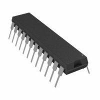
AD7890BN-10 Analog Devices Inc, AD7890BN-10 Datasheet - Page 5

AD7890BN-10
Manufacturer Part Number
AD7890BN-10
Description
IC DAS 12BIT 8CH 24-DIP
Manufacturer
Analog Devices Inc
Type
Data Acquisition System (DAS)r
Datasheet
1.AD7890ARZ-10.pdf
(28 pages)
Specifications of AD7890BN-10
Mounting Type
Through Hole
Package / Case
24-DIP (0.300", 7.62mm)
Rohs Status
RoHS non-compliant
Resolution (bits)
12 b
Sampling Rate (per Second)
117k
Data Interface
Serial
Voltage Supply Source
Single Supply
Voltage - Supply
±10V
Operating Temperature
-40°C ~ 85°C
Supply Voltage
5V
No. Of Bits
12 Bit
Interface Type
Serial
Lead Free Status / RoHS Status
TIMING SPECIFICATIONS
V
Parameter
f
t
t
tr
tf
t
t
Self-Clocking Mode
t
t
t
t
t
t
t
t
t
t
t
t
External Clocking Mode
t
t
t
t
t
t
t
t
t
t
t
t
1
2
3
4
5
6
CLKIN
CLKIN IN LO
CLK IN HI
CONVERT
CST
1
2
3
4
5
6
7
8
9
10
11
12
13
14
15
16
17
18
19
19A
20
21
22
23
Sample tested at −25°C to ensure compliance. All input signals are specified with tr = tf = 5 ns (10% to 90% of 5 V) and timed from a voltage level of 1.6 V.
See Figure 10 to Figure 13.
The AD7890 is production tested with f
Specified using 10% and 90% points on waveform of interest.
These numbers are measured with the load circuit of Figure 2 and defined as the time required for the output to cross 0.8 V or 2.4 V.
These numbers are derived from the measured time taken by the data output to change 0.5 V when loaded with the circuit of Figure 2. The measured number is then
extrapolated back to remove effects of charging or discharging the 50 pF capacitor. This means that the times quoted in the timing characteristics are the true bus
relinquish times of the part and as such are independent of external bus loading capacitances.
4
5
4
5
6
DD
5
5
6
6
3
= 5 V ± 5%, AGND = DGND = 0 V, REF IN = 2.5 V, f
1 , 2
Limit at T
100
2.5
0.3 × t
0 3 × t
25
25
5.9
100
t
25
t
t
20
40
50
0
t
0
20
10
20
20
40
50
50
35
20
50
90
20
10
15
40
CLK IN HI
CLK IN HI
CLK IN LO
CLK IN
+ 50
CLK IN
CLK IN
CLK IN
+ 50
MIN
at 2.5 MHz. It is guaranteed by characterization to operate at 100 kHz.
, T
MAX
Figure 2. Load Circuit for Access Time and Bus Relinquish Time
(A, B, S Versions)
TO OUTPUT
PIN
CLK IN
50pF
Rev. C | Page 5 of 28
= 2.5 MHz external, MUX OUT connected to SHA IN.
Unit
kHz min
MHz max
ns min
ns min
ns max
ns max
μs max
ns min
ns max
ns max
ns nom
ns nom
ns max
ns max
ns max
ns min
ns max
ns min
ns min
ns min
ns min
ns min
ns max
ns min
ns min
ns max
ns min
ns max
ns max
ns min
ns min
ns min
ns min
1.6mA
200µA
Conditions/Comments
Master Clock Frequency. For specified performance.
Conversion Time.
SCLK Rising Edge to Data Valid Delay.
Bus Relinquish Time after Rising Edge of SCLK.
Data Valid to SCLK Falling Edge Setup Time.
Data Valid to SCLK Falling Edge Hold Time.
SCLK Rising Edge to Data Valid Delay.
Bus Relinquish Time after Rising Edge of SCLK.
Data Valid to SCLK Falling Edge Setup Time.
Data Valid to SCLK Falling Edge Hold Time.
Master Clock Input Low Time.
Master Clock Input High Time.
Digital Output Rise Time. Typically 10 ns.
Digital Output Fall Time. Typically 10 ns.
CONVST Pulse Width.
RFS Low to SCLK Falling Edge.
RFS Low to Data Valid Delay.
SCLK High Pulse Width.
SCLK Low Pulse Width.
SCLK Rising Edge to RFS Delay.
TFS Low to SCLK Falling Edge.
Data Valid to TFS Falling Edge Setup Time (A2 Address Bit).
TFS to SCLK Falling Edge Hold Time.
RFS Low to SCLK Falling Edge Setup Time.
RFS Low to Data Valid Delay.
SCLK High Pulse Width.
SCLK Low Pulse Width.
RFS to SCLK Falling Edge Hold Time.
Bus Relinquish Time after Rising Edge of RFS.
TFS Low to SCLK Falling Edge Setup Time.
TFS to SCLK Falling Edge Hold Time.
2.1V
AD7890


