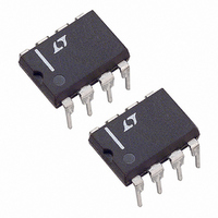
LTC1092ACN8 Linear Technology, LTC1092ACN8 Datasheet - Page 4

LTC1092ACN8
Manufacturer Part Number
LTC1092ACN8
Description
IC DAS SERIAL I/O 1CH 10BIT 8DIP
Manufacturer
Linear Technology
Type
Data Acquisition System (DAS), ADCr
Datasheet
1.LTC1091CN8PBF.pdf
(32 pages)
Specifications of LTC1092ACN8
Resolution (bits)
10 b
Data Interface
Serial
Voltage Supply Source
Single Supply
Voltage - Supply
4.5 V ~ 10 V
Operating Temperature
-40°C ~ 85°C
Mounting Type
Through Hole
Package / Case
8-DIP (0.300", 7.62mm)
Lead Free Status / RoHS Status
Contains lead / RoHS non-compliant
Sampling Rate (per Second)
-
Available stocks
Company
Part Number
Manufacturer
Quantity
Price
AC CHARACTERISTICS
The denotes specifications which apply over the full operating temperature range, otherwise specifications are T
SYMBOL PARAMETER
t
t
t
t
t
t
t
t
C
The
Note 1: Absolute Maximum Ratings are those values beyond which the life
of a device may be impaired.
Note 2: All voltage values are with respect to ground with DGND, AGND,
GND and REF
connected to the AGND pin on the LTC1093. DGND, AGND, REF
are internally connected to the GND pin on the LTC1091/LTC1092.
Note 3: V
– 5V for bipolar mode, CLK = 0.5MHz unless otherwise specified.
Note 4: These specs apply for both unipolar (LTC1091/LTC1092/LTC1093/
LTC1094) and bipolar (LTC1093/LTC1094 only) modes. In bipolar mode,
one LSB is equal to the bipolar input span (2V
example, when V
Note 5: Linearity error is specified between the actual end points of the
A/D transfer curve.
SYMBOL PARAMETER
V
V
I
I
V
V
I
I
I
I
I
I
4
LTC1091/LTC1092
LTC1093/LTC1094
DIGITAL A D
SMPL
CONV
dDO
dis
en
hDO
f
r
IH
IL
OZ
SOURCE
SINK
CC
REF
–
IN
IH
IL
OH
OL
denotes specifications which apply over the full operating temperature range, otherwise specifications are T
CC
High Level Input Voltage
Low Level Input Voltage
High Level Input Current
Low Level Input Current
High Level Output Voltage
Low Level Output Voltage
Hi-Z Output Leakage
Output Source Current
Output Sink Current
Positive Supply Current
Reference Current
Negative Supply Current
Analog Input Sample Time
Conversion Time
Delay Time, CLK to D
Delay Time, CS to D
Delay Time, CLK to D
Time Output Data Remains Valid After SCLK
D
D
Input Capacitance
= 5V, V
OUT
OUT
–
wired together (unless otherwise noted). REF
REF
Fall Time
Rise Time
REF
= 5V, 1LSB (bipolar) = 2(5V)/1024 = 9.77mV.
+
U
= 5V, V
REF
DC
OUT
OUT
OUT
–
= 0V, V
Hi-Z
Data Valid
Enabled
ELECTRICAL C
CONDITIONS
V
V
V
V
V
V
V
V
V
V
V
LTC1091, CS High
LTC1092/LTC1093/LTC1094, CS High, REF
LTC1092/LTC1093/LTC1094, V
LTC1093/LTC1094, CS High, V
CC
CC
IN
IN
CC
CC
CC
OUT
OUT
OUT
OUT
–
= V
= 0V
= 5.25V
= 4.75V
= 4.75V, I
= 4.75V, I
= 4.75V, I
REF
= 0V for unipolar mode and
= V
= 0V, CS High
= 0V
= V
CC
) divided by 1024. For
CC
CC
, CS High
OUT
OUT
OUT
= 10 A
= 360 A
= 1.6mA
CONDITIONS
See Operating Sequence
See Operating Sequence
See Test Circuits
See Test Circuits
See Test Circuits
See Test Circuits
See Test Circuits
Analog Inputs On-Channel
Analog Inputs Off-Channel
Digital Inputs
–
is internally
–
and V
HARA TER STICS
–
REF
–
= – 5V
= 5V
Note 6: Total unadjusted error includes offset, full scale, linearity,
multiplexer and hold step errors.
Note 7: Two on-chip diodes are tied to each reference and analog input
which will conduct for reference or analog input voltages one diode drop
below V
V
this input diode to conduct, especially at elevated temperatures, and cause
errors for inputs near full scale. This spec allows 50mV forward bias of
either diode. This means that as long as the reference or analog input does
not exceed the supply voltage by more than 50mV, the output code will be
correct. To achieve an absolute 0V to 5V input voltage range will therefore
require a minimum supply voltage of 4.950V over initial tolerance,
temperature variations and loading.
Note 8: Channel leakage current is measured after the channel selection.
CC
C
+
levels (4.5V), as high level reference or analog inputs (5V) can cause
Open
–
or one diode drop above V
I
LTC1091A/LTC1092A/LTC1093A/LTC1094A
LTC1091/LTC1092/LTC1093/LTC1094
MIN
LTC1091A/LTC1092A/LTC1093A/LTC1094A
LTC1091/LTC1092/LTC1093/LTC1094
MIN
2.0
2.4
CC
TYP
400
180
160
150
1.5
10
90
60
65
5
5
. Be careful during testing at low
TYP
–10
4.7
4.0
1.5
1.0
0.5
10
1
A
A
MAX
850
450
450
300
300
= 25 C. (Note 3)
= 25 C. (Note 3)
MAX
–2.5
0.8
2.5
0.4
3.5
2.5
1.0
–3
50
3
CLK Cycles
CLK Cycles
UNITS
UNITS
mA
mA
mA
mA
mA
ns
ns
ns
ns
ns
ns
pF
pF
pF
V
V
A
A
V
V
V
A
A
A


