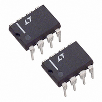
LTC1291DCN8 Linear Technology, LTC1291DCN8 Datasheet - Page 2

LTC1291DCN8
Manufacturer Part Number
LTC1291DCN8
Description
IC DATA ACQ SYSTEM 12BIT 8-DIP
Manufacturer
Linear Technology
Type
Data Acquisition System (DAS)r
Datasheet
1.LTC1291DCN8PBF.pdf
(20 pages)
Specifications of LTC1291DCN8
Resolution (bits)
12 b
Data Interface
Serial, Parallel
Voltage Supply Source
Single Supply
Voltage - Supply
5V
Operating Temperature
0°C ~ 70°C
Mounting Type
Through Hole
Package / Case
8-DIP (0.300", 7.62mm)
Lead Free Status / RoHS Status
Contains lead / RoHS non-compliant
Sampling Rate (per Second)
-
Available stocks
Company
Part Number
Manufacturer
Quantity
Price
Company:
Part Number:
LTC1291DCN8
Manufacturer:
LT
Quantity:
5 510
Company:
Part Number:
LTC1291DCN8
Manufacturer:
XILI
Quantity:
5 510
LTC1291
A
(Notes 1 and 2)
CO VERTER A D
otherwise specifications are at T
Supply Voltage (V
Voltage
Power Dissipation ............................................. 500mW
Operating Temperature Range
Storage Temperature Range ................. –65 C to 150 C
Lead Temperature (Soldering, 10 sec)................. 300 C
AC CHARACTERISTICS
SYMBOL
f
t
t
t
t
PARAMETER
Offset Error
Linearity Error (INL)
Gain Error
Minimum Resolution for which No
Missing Codes are Guaranteed
Analog Input Range
On Channel Leakage Current
Off Channel Lekage Current
2
which apply over the full operating temperature range, otherwise specifications are at T
CLK
SMPL
CONV
CYC
dDO
(Note 8)
(Note 8)
BSOLUTE
Analog Inputs ............................ –0.3V to V
Digital Inputs ........................................ –0.3V to 12V
Digital Outputs .......................... –0.3V to V
LTC1291BC, LTC1291CC,
LTC1291DC ............................................ 0 C to 70 C
U
PARAMETER
Clock Frequency
Analog Input Sample Time
Conversion Time
Total Cycle Time
Delay Time, CLK to D
CC
W
) to GND .................................. 12V
A
U W
XI
W
OUT
A
= 25 C. (Note 3)
Data Valid
U
CONDITIONS
(Note 4)
(Note 4 & 5)
(Note 4)
(Note 7)
On Channel = 5V
Off Channel = 0V
On Channel = 0V
Off Channel = 5V
On Channel = 5V
Off Channel = 0V
On Channel = 0V
Off Channel = 5V
W
ULTIPLEXER CHARACTERISTICS
The
R
A
denotes the specifications which apply over the full operating temperature range,
TI
CONDITIONS
V
See Operating Sequence
See Operating Sequence
See Operating Sequence (Note 6)
See Test Circuits
CC
U
= 5V (Note 6)
CC
CC
G
+ 0.3V
+ 0.3V
S
MIN
LTC1291B
PACKAGE/ORDER I FOR ATIO
Consult LTC Marketing for parts specified with wider operating temperature ranges.
TYP MAX
GND
CH0
CH1
CS
T
T
JMAX
JMAX
12
1
3
4
2
3.0
0.5
1.0
8-LEAD CERAMIC DIP
8-LEAD PLASTIC DIP
1
1
1
1
= 100 C,
= 150 C,
N8 PACKAGE
J8 PACKAGE
TOP VIEW
– 0.05V to V
MIN
Consider N8 Package for Alternate Source
OBSOLETE PACKAGE
A
JA
JA
LTC1291C
= 25 C. (Note 3)
= 130 C/ W (N8)
= 100 C/ W (J8)
LTC1291B/LTC1291C/LTC1291D
TYP MAX
8
7
6
5
CC
(Note 9)
+ 500ns
18 CLK
MIN
V
CLK
D
D
+ 0.05V
CC
IN
OUT
The
12
3.0
0.5
2.0
1
1
1
1
(V
REF
)
TYP
160
2.5
12
denotes the specifications
U
MIN
LTC1291D
MAX
LTC1291BCN8
LTC1291CCN8
LTC1291DCN8
LTC1291BCJ8
LTC1291CCJ8
LTC1291DCJ8
TYP MAX
300
1.0
ORDER PART
NUMBER
W
0.75
12
3.0
4.0
1
1
1
1
CLK Cycles
CLK Cycles
UNITS
Cycles
UNITS
1291fa
U
MHz
LSB
LSB
LSB
Bits
ns
V
A
A
A
A


