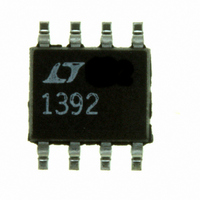
LTC1392CS8 Linear Technology, LTC1392CS8 Datasheet - Page 7

LTC1392CS8
Manufacturer Part Number
LTC1392CS8
Description
IC DATA ACQ SYSTEM 10BIT 8-SOIC
Manufacturer
Linear Technology
Type
Data Acquisition System (DAS)r
Datasheet
1.LTC1392CN8PBF.pdf
(12 pages)
Specifications of LTC1392CS8
Resolution (bits)
10 b
Sampling Rate (per Second)
25k
Data Interface
Serial
Voltage Supply Source
Single Supply
Voltage - Supply
4.5 V ~ 6 V
Operating Temperature
0°C ~ 70°C
Mounting Type
Surface Mount
Package / Case
8-SOIC (3.9mm Width)
Lead Free Status / RoHS Status
Contains lead / RoHS non-compliant
Available stocks
Company
Part Number
Manufacturer
Quantity
Price
Company:
Part Number:
LTC1392CS8
Manufacturer:
LNEAR
Quantity:
10 000
Company:
Part Number:
LTC1392CS8
Manufacturer:
LT
Quantity:
10 000
Part Number:
LTC1392CS8
Manufacturer:
LINEAR/凌特
Quantity:
20 000
Part Number:
LTC1392CS8#PBF
Manufacturer:
LINEAR/凌特
Quantity:
20 000
Company:
Part Number:
LTC1392CS8#TR
Manufacturer:
LINEAR
Quantity:
4 702
Company:
Part Number:
LTC1392CS8#TRPBF
Manufacturer:
LINEAR
Quantity:
6 567
APPLICATIONS
MSB-First Data (MSBF = 1)
D
D
temperature measurement or a 10 s delay for other mea-
surements, followed by a 4-bit input word which config-
ures the LTC1392 for the current conversion. This data
word is shifted into the D
shifting in any data and the D
three-state to an output pin. A null bit and the result of the
current conversion are serially transmitted on the falling
CLK edge onto the D
can be either MSB-first sequence or MSB-first sequence
followed by an LSB-first sequence. This provides easy
interface to MSB- or LSB-first serial ports. Bringing CS
high resets the LTC1392 for the next data exchange.
INPUT DATA WORD
Data transfer is initiated by a falling chip select (CS) signal.
After CS falls, the LTC1392 looks for a start bit. Once the
start bit is received, the next three bits are shifted into the
CLK
CLK
D
OUT
D
OUT
CS
CS
IN
IN
t
t
WAKEUP
WAKEUP
Hi-Z
Hi-Z
START
START
t
t
suCS
suCS
SEL1 SEL0
SEL1 SEL0
t
t
U
SMPL
SMPL
MSBF
MSBF
OUT
IN
INFORMATION
line. The format of the A/D result
U
input. D
B9
B9
OUT
B8
B8
B7
B7
IN
pin is configured from
W
is then disabled from
B6
B6
t
t
CONV
CONV
B5
B5
B4
B4
B3
B3
U
B2
B2
B1
B1
t
t
CYC
CYC
Figure 1
B0
B0
B1
D
conversion. Further inputs on the D
ignored until the next CS cycle. The four bits of the input
word are defined as follows:
Start Bit
The first “logic one” clocked into the D
goes low is the Start Bit. The Start Bit initiates the data
transfer and all leading zeros which precede this logical
one will be ignored. After the Start Bit is received the
remaining bits of the input word will be clocked in. Further
input on the D
cycle.
IN
B2
input which configures the LTC1392 and starts the
B3
BIT 3
Start
B4
B5
B6
IN
FILLED WITH ZEROS
pin are then ignored until the next CS
B7
Select 1
BIT 2
B8
B9
FILLED WITH ZEROS
Select 0
BIT 1
IN
IN
input are then
LTC1392
input after CS
MSBF
BIT 0
Hi-Z
Hi-Z
LTC1392 • F01
7


