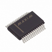
MAX127BEAI+ Maxim Integrated Products, MAX127BEAI+ Datasheet - Page 15

MAX127BEAI+
Manufacturer Part Number
MAX127BEAI+
Description
IC DAS 12BIT 2-WIRE 28-SSOP
Manufacturer
Maxim Integrated Products
Type
Data Acquisition System (DAS)r
Datasheet
1.MAX128BCAI.pdf
(16 pages)
Specifications of MAX127BEAI+
Resolution (bits)
12 b
Sampling Rate (per Second)
8k
Data Interface
Serial
Voltage Supply Source
Single Supply
Voltage - Supply
4.75 V ~ 5.25 V
Operating Temperature
-40°C ~ 85°C
Mounting Type
Surface Mount
Package / Case
28-SSOP
Number Of Adc Inputs
8
Architecture
SAR
Conversion Rate
8 KSPs
Resolution
12 bit
Interface Type
I2C
Voltage Reference
Internal 4.096 V or External
Supply Voltage (max)
5 V
Mounting Style
SMD/SMT
Input Voltage
10 V
Lead Free Status / RoHS Status
Lead free / RoHS Compliant
Output data coding for the MAX127/MAX128 is binary
in unipolar mode with 1LSB = (FS/4096) and
two’s complement binary in bipolar mode with 1LSB =
[(2 x FS ) / 4096]. Code transitions occur halfway
between successive-integer LSB values. Figures 13a
and 13b show the input/output (I/O) transfer functions
for unipolar and bipolar operations, respectively. For
full-scale (FS) values, refer to Table 3.
Figure 13a. Unipolar Transfer Function
Figure 13b. Bipolar Transfer Function
011... 111
011... 110
000... 001
000... 000
111... 111
100... 010
100... 001
100... 000
00... 011
00... 010
00... 001
00... 000
11... 111
11... 110
11... 101
OUTPUT CODE
OUTPUT CODE
0
-FS
1
2
______________________________________________________________________________________
3
INPUT VOLTAGE (LSB)
INPUT VOLTAGE (LSB)
0
FULL-SCALE
TRANSITION
Transfer Function
Multirange, +5V, 12-Bit DAS with
FS -
+FS - 1 LSB
3
/
2
LSB
1 LSB =
1 LSB =
FS
4096
2 FS
FS
4096
Careful printed circuit board layout is essential for best
system performance. For best performance, use a
ground plane. To reduce crosstalk and noise injection,
keep analog and digital signals separate. Connect ana-
log grounds and DGND in a star configuration to
AGND. For noise-free operation, ensure the ground
return from AGND to the supply ground is low imped-
ance and as short as possible. Connect the logic
grounds directly to the supply ground. Bypass V
0.1µF and 4.7µF capacitors to AGND to minimize high-
and low-frequency fluctuations. If the supply is exces-
sively noisy, connect a 5Ω resistor between the supply
and V
Figure 14. Power-Supply Grounding Connection
2-Wire Serial Interface
* OPTIONAL
** CONNECT AGND AND DGND WITH A GROUND PLANE OR A SHORT TRACE.
R* = 5
DD
+5V
V
, as shown in Figure 14.
DD
Layout, Grounding, and Bypassing
4.7 F
0.1 F
AGND
MAX127
MAX128
**
SUPPLY
DGND
+5V
CIRCUITRY
DIGITAL
GND
DGND
DD
with
15


