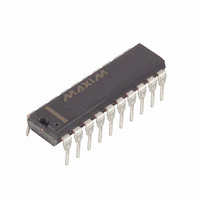
MAX192AEPP+ Maxim Integrated Products, MAX192AEPP+ Datasheet - Page 4

MAX192AEPP+
Manufacturer Part Number
MAX192AEPP+
Description
IC ADC 10BIT SERIAL 20-DIP
Manufacturer
Maxim Integrated Products
Type
Data Acquisition System (DAS), ADCr
Datasheet
1.MAX192BEWP.pdf
(24 pages)
Specifications of MAX192AEPP+
Resolution (bits)
10 b
Sampling Rate (per Second)
133k
Data Interface
Serial
Voltage Supply Source
Single Supply
Voltage - Supply
±5V
Operating Temperature
-40°C ~ 85°C
Mounting Type
Through Hole
Package / Case
20-DIP (0.300", 7.62mm)
Lead Free Status / RoHS Status
Lead free / RoHS Compliant
ELECTRICAL CHARACTERISTICS (continued)
(V
T
Note 1: Tested at V
Note 2: Relative accuracy is the deviation of the analog value at any code from its theoretical value after the full-scale range has
Note 3: Grounded on-channel; sine wave applied to all off channels.
Note 4: Conversion time defined as the number of clock cycles times the clock period; clock has 50% duty cycle.
Note 5: Guaranteed by design. Not subject to production testing.
Note 6: The common-mode range for the analog inputs is from AGND to V
Note 7: Sample tested to 0.1% AQL.
Note 8: External load should not change during conversion for specified accuracy.
Note 9: Measured at V
Low-Power, 8-Channel,
Serial 10-Bit ADC
4
A
EXTERNAL REFERENCE AT REFADJ
DIGITAL INPUTS (DIN, SCLK,
DIGITAL OUTPUTS (DOUT, SSTRB)
POWER REQUIREMENTS
DIN,SCLK, CS Input High Voltage
DIN,SCLK, CS Input Low Voltage
DIN, SCLK, CS Input Hysteresis
DIN, SCLK, CS Input Leakage
DIN, SCLK, CS Input Capacitance
SHDN Input High Voltage
SHDN Input Low Voltage
SHDN Input Current, High
SHDN Input Current, Low
SHDN Input Mid Voltage
SHDN Voltage, Floating
SHDN Max Allowed Leakage,
Mid Input
Output Voltage Low
Output Voltage High
Three-State Leakage Current
Three-State Leakage Capacitance
Positive Supply Voltage
Positive Supply Current
Positive Supply Rejection
(Note 9)
DD
= T
_______________________________________________________________________________________
= 5V ±5%, f
MIN
been calibrated.
PARAMETER
to T
MAX,
CLK
unless otherwise noted. Typical values are at T
DD
= 2.0MHz, external clock (50% duty cycle), 15 clocks/conversion cycle (133ksps), 4.7µF capacitor at VREF pin,
= 5.0V; single-ended, unipolar.
SUPPLY
+ 5% and V
–
C
—
S
–
SYMBOL
,
V
C
–
S
V
V
V
—
V
V
V
PSR
I
V
V
C
I
HYST
V
I
I
INH
INL
OUT
H
INH
INH
DD
INL
INL
FLT
I
IN
OH
DD
—
OL
IM
IN
L
D
—
SUPPLY
N
–
)
V
(Note 5)
SHDN = V
SHDN = 0V
SHDN = open
SHDN = open
I
I
I
CS = 5V
CS = 5V (Note 5)
Operating mode
Fast power-down
Full power-down
V
full-scale input
SINK
SINK
SOURCE
IN
DD
- 5% only.
= 0V or V
= 5V ±5%; external reference, 4.096V;
= 5mA
= 16mA
= 1mA
DD
DD
CONDITIONS
A
= +25°C.)
DD
.
V
DD
MIN
-100
-4.0
2.4
1.5
4
- 0.5
5 ±5%
±0.06
TYP
0.15
2.75
0.3
1.5
30
2
V
DD
MAX
±0.5
100
±10
0.8
0.5
4.0
0.4
2.5
±1
15
15
70
10
- 1.5
UNITS
mA
mV
µA
pF
µA
µA
nA
µA
pF
µA
V
V
V
V
V
V
V
V
V
V


