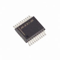
MAX1409CAP+ Maxim Integrated Products, MAX1409CAP+ Datasheet - Page 45

MAX1409CAP+
Manufacturer Part Number
MAX1409CAP+
Description
IC DAS 16BIT LP 20-SSOP
Manufacturer
Maxim Integrated Products
Type
Data Acquisition System (DAS)r
Datasheet
1.MAX1409CAP.pdf
(48 pages)
Specifications of MAX1409CAP+
Resolution (bits)
16 b
Sampling Rate (per Second)
60
Data Interface
Serial
Voltage Supply Source
Analog and Digital
Voltage - Supply
2.7 V ~ 3.6 V
Operating Temperature
0°C ~ 70°C
Mounting Type
Surface Mount
Package / Case
20-SSOP
Lead Free Status / RoHS Status
Lead free / RoHS Compliant
Figure 28 shows a thermocouple connected to the dif-
ferential inputs of the MAX1407/MAX1408/MAX1409/
MAX1414. In this application, the internal buffers are
enabled to allow for the decoupling shown at the input.
The decoupling eliminates noise pickup from the ther-
mocouple. With the internal buffers enabled, the input
common-mode range is reduced so the IN2 input is
biased to the internal reference voltage at +1.25V. When
the buffer is enabled, the IN1 input is limited to +1.4V.
Connect the differential inputs of the MAX1407/
MAX1408/MAX1409/MAX1414 to the bridge network of
the strain gauge as shown in Figure 29. When connect-
ed to the internal reference, the ADC can resolve below
10µV at the differential inputs. The internal buffers pro-
vide a high input impedance as long as the signal is
within the reduced common-mode range of the input
buffers. The bridge may also be driven directly from the
supply voltage. In this configuration, the ADC first mea-
sures the supply voltage and then the differential input
in sequence, and then calculates the ratio.
For best performance, use printed circuit boards with
separate analog and digital ground planes. The device
perfomance will be highly degraded when using wire-
wrap boards.
Design the printed circuit board so that the analog and
digital sections are separated and confined to different
areas of the board. Join the digital and analog ground
planes at one point. If the MAX1407/MAX1408/
MAX1409/MAX1414 is the only device requiring an
AGND to DGND connection, then the ground planes
should be connected at the AGND pin of the MAX1407/
Figure 29. Strain-Gauge Application Circuit
Low-Power, 16-Bit Multichannel DAS with
Internal Reference,10-Bit DACs, and RTC
______________________________________________________________________________________
Thermocouple Measurement
R
R
D
A
REF OR AV
Strain-Gauge Operation
Grounding and Layout
DD
R
R
B
C
DRDY NOT AVAILABLE ON THE MAX1409
IN0
IN1
MAX1407
MAX1408
MAX1414
MUX
MUX
8:1
8:1
16-BIT ADC
WAKE-UP
CMP
REF
MAX1408/MAX1409/MAX1414. In systems where multi-
ple devices require AGND to DGND connections, the
connection should still be made at only one point. Make
the star ground as close to the MAX1407/MAX1408/
MAX1409/MAX1414 as possible.
Avoid running digital lines under the device because
these may couple noise onto the die. Run the analog
ground plane under the MAX1407/MAX1408/
MAX1409/MAX1414 to minimize coupling of digital
noise. Make the power-supply lines to the MAX1407/
MAX1408/MAX1409/MAX1414 as wide as possible to
provide low-impedance paths and reduce the effects of
glitches on the power-supply line.
Shield fast switching signals such as clocks with digital
ground to avoid radiating noise to other sections of the
board. Avoid running clock signals near the analog
inputs. Avoid crossover of digital and analog signals.
Traces on opposite sides of the board should run at
right angles to each other. This will reduce the effects
of feedthrough on the board. A microstrip technique is
best, but is not always possible with double-sided
boards. In this technique, the component side of the
board is dedicated to ground planes while signals are
placed on the solder side.
Good coupling is important when using high-resolution
ADCs. Decouple all analog supplies with 1µF capaci-
tors in parallel with 0.1µF HF ceramic capacitors to
AGND. Place these components as close to the device
as possible to achieve the best decoupling.
Since it is possible for noise to be coupled onto the
crystal pins, care must be taken when placing the
external crystal on a PC board layout. It is very impor-
tant to follow a few basic layout guidelines concerning
BAND
GAP
GENERATOR
INTERRUPT
BUF
DRDY
INT
4.7µF
REF
Crystal Layout
45


