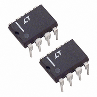
LTC1287CCN8 Linear Technology, LTC1287CCN8 Datasheet - Page 13

LTC1287CCN8
Manufacturer Part Number
LTC1287CCN8
Description
IC DATA ACQ SYS 12BIT 3V 8-DIP
Manufacturer
Linear Technology
Type
Data Acquisition System (DAS)r
Datasheet
1.LTC1287CCN8.pdf
(16 pages)
Specifications of LTC1287CCN8
Resolution (bits)
12 b
Sampling Rate (per Second)
30k
Data Interface
Serial, Parallel
Voltage Supply Source
Single Supply
Voltage - Supply
3V
Operating Temperature
0°C ~ 70°C
Mounting Type
Through Hole
Package / Case
8-DIP (0.300", 7.62mm)
Lead Free Status / RoHS Status
Contains lead / RoHS non-compliant
Available stocks
Company
Part Number
Manufacturer
Quantity
Price
Company:
Part Number:
LTC1287CCN8
Manufacturer:
TI
Quantity:
190
A
conversion (every CLK cycle) a capacitive current spike
will be generated on the reference pin by the A/D. These
current spikes settle quickly and do not cause a prob-
lem. If slow settling circuitry is used to drive the
reference input, take care to insure that transients
caused by these current spikes settle completely during
each bit test of the conversion.
PPLICATI
Figure 14. Poor Reference Settling Can Cause A/D Errors
Figure 12. Reference Input Equivalent Circuit
R
V
Figure 13. Adequate Reference Settling
OUT
REF
O
REF+
GND
14
13
U
HORIZONTAL: 1 s/DIV
HORIZONTAL: 10 s/DIV
S
I FOR ATIO
U
EVERY CLK CYCLE
R
ON
W
8pF – 40pF
LTC1287
LTC 1287 F12
U
Figures 13 and 14 show examples of both adequate and
poor settling. Using a slower CLK will allow more time
for the reference to settle. Even at the maximum CLK
rate of 500kHz most references and op amps can be
made to settle within the 2 s bit time. For example an
LT1790 with a 4.7 F bypass capacitor will settle
adequately.
Reduced Reference Operation
The effective resolution of the LTC1287 can be in-
creased by reducing the input span of the converter.
The LTC1287 exhibits good linearity over a range of
reference voltages (seeTypical Performance Charac-
teristics curves of Change in Linearity vs Reference
Voltage). Care must be taken when operating at low
values of V
the resulting higher accuracy requirement placed on
the converter. Offset and Noise are factors that must be
considered when operating at low V
Offset with Reduced V
The offset of the LTC1287 has a larger effect on the
output code when the A/D is operated with a reduced
reference voltage. The offset (which is typically a fixed
voltage) becomes a larger fraction of an LSB as the size
of the LSB is reduced. The Typical Performance Charac-
teristics curve of Unadjusted Offset Error vs Reference
Voltage shows how offset in LSBs is related to reference
voltage for a typical value of V
0.1mV, which is 0.2LSB with a 2.5V reference becomes
0.4LSB with a 1.25 reference. If this offset is unaccept-
able, it can be corrected digitally by the receiving system
or by offsetting the –IN input to the LTC1287.
Noise with Reduced V
The total input referred noise of the LTC1287 can be
reduced to approximately 200 V peak-to-peak using a
ground plane, good bypassing, good layout techniques
and minimizing noise on the reference inputs. This
noise is insignificant with a 2.5V reference input but will
become a larger fraction of an LSB as the size of the LSB
is reduced. The Typical Performance Characteristics
REF
because of the reduced LSB step size and
REF
REF
OS
. For example a V
REF
LTC1287
values.
13
OS
1287fa
of


