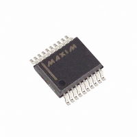
MAX192BEAP+ Maxim Integrated Products, MAX192BEAP+ Datasheet - Page 13

MAX192BEAP+
Manufacturer Part Number
MAX192BEAP+
Description
IC ADC 10BIT SERIAL 20-SSOP
Manufacturer
Maxim Integrated Products
Type
Data Acquisition System (DAS), ADCr
Datasheet
1.MAX192BEWP.pdf
(24 pages)
Specifications of MAX192BEAP+
Resolution (bits)
10 b
Sampling Rate (per Second)
133k
Data Interface
Serial
Voltage Supply Source
Single Supply
Voltage - Supply
±5V
Operating Temperature
-40°C ~ 85°C
Mounting Type
Surface Mount
Package / Case
20-SSOP
Package
20SSOP
Resolution
10 Bit
Sampling Rate
133 KSPS
Architecture
SAR
Number Of Adcs
1
Number Of Analog Inputs
8|4
Digital Interface Type
Serial (4-Wire, SPI, QSPI, Microwire)
Input Type
Voltage
Polarity Of Input Voltage
Unipolar|Bipolar
Conversion Rate
133 KSPs
Interface Type
Serial
Voltage Reference
Internal 4.096 V or External
Supply Voltage (max)
5 V
Maximum Power Dissipation
640 mW
Maximum Operating Temperature
+ 85 C
Mounting Style
SMD/SMT
Minimum Operating Temperature
- 40 C
Lead Free Status / RoHS Status
Lead free / RoHS Compliant
Most microcontrollers require that conversions occur in
multiples of 8 SCLK clocks; 16 clocks per conversion
will typically be the fastest that a microcontroller can
drive the MAX192. Figure 11b shows the serial-inter-
face timing necessary to perform a conversion every 16
SCLK cycles in external clock mode.
__________ Applications Information
When power is first applied and if SHDN is not pulled
low, internal power-on reset circuitry will activate the
MAX192 in internal clock mode, ready to convert with
SSTRB = high. After the power supplies have been sta-
bilized, the internal reset time is 100µs and no conver-
sions should be performed during this phase. SSTRB is
high on power-up and, if CS is low, the first logical 1 on
DIN will be interpreted as a start bit. Until a conversion
takes place, DOUT will shift out zeros.
Figure 8. External Clock Mode SSTRB Detailed Timing
Figure 9. Internal Clock Mode Timing
SSTRB
SCLK
CS
SSTRB
DOUT
A/D STATE
SCLK
DIN
CS
START SEL2 SEL1 SEL0
______________________________________________________________________________________
1
2
3
IDLE
t
SDV
4
UNI/
BIP
5
1.5µs (CLK = 2MHz)
Power-On Reset
SGL/
DIF
ACQUISITION
6
PD1
7
PD0
8
PD0 CLOCKED IN
CONVERSION
10µs MAX
t
CONV
9
In addition to its shutdown function, the SHDN pin also
selects internal or external compensation. The compen-
sation affects both power-up time and maximum conver-
sion speed. Compensated or not, the minimum clock
rate is 100kHz due to droop on the sample-and-hold.
To select external compensation, float SHDN. See the
Typical Operating Circuit , which uses a 4.7µF capacitor
at VREF. A value of 4.7µF or greater ensures stability
and allows operation of the converter at the full clock
speed of 2MHz. External compensation increases
power-up time (see the Choosing Power-Down Mode
section, and Table 5).
Internal compensation requires no external capacitor at
VREF, and is selected by pulling SHDN high. Internal
compensation allows for shortest power-up times, but is
only available using an external clock and reduces the
maximum clock rate to 400kHz.
Low-Power, 8-Channel,
MSB
t
SSTRB
B9
IDLE
10
B8
11
B7
12
Serial 10-Bit ADC
Reference-Buffer Compensation
18
t
SSTRB
LSB
B0
19
S1
20
S0
21
FILLED WITH
ZEROS
22
23
t
STR
24
13


