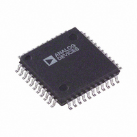
AD2S1200WSTZ Analog Devices Inc, AD2S1200WSTZ Datasheet - Page 20

AD2S1200WSTZ
Manufacturer Part Number
AD2S1200WSTZ
Description
IC R/D CONV W/REF OSCIL 44-LQFP
Manufacturer
Analog Devices Inc
Type
R/D Converterr
Datasheet
1.AD2S1200.pdf
(24 pages)
Specifications of AD2S1200WSTZ
Resolution (bits)
12 b
Data Interface
Serial, Parallel
Voltage Supply Source
Analog and Digital
Voltage - Supply
4.75 V ~ 5.25 V
Operating Temperature
-40°C ~ 125°C
Mounting Type
Surface Mount
Package / Case
44-LQFP
Input Channel Type
Differential
Supply Voltage Range - Analog
4.75V To 5.25V
Supply Voltage Range - Digital
4.75V To 5.25V
Lead Free Status / RoHS Status
Lead free / RoHS Compliant
For Use With
EVAL-AD2S1200CBZ - BOARD EVAL FOR AD2S1200
Sampling Rate (per Second)
-
Lead Free Status / RoHS Status
Lead free / RoHS Compliant, Lead free / RoHS Compliant
Available stocks
Company
Part Number
Manufacturer
Quantity
Price
Company:
Part Number:
AD2S1200WSTZ
Manufacturer:
Analog Devices Inc
Quantity:
135
Company:
Part Number:
AD2S1200WSTZ
Manufacturer:
ADI
Quantity:
276
Company:
Part Number:
AD2S1200WSTZ
Manufacturer:
Analog Devices Inc
Quantity:
10 000
AD2S1200
CLOCK REQUIREMENTS
To achieve the specified dynamic performance, an external
crystal of 8.192 MHz must be used at the CLKIN, XTALOUT
pins. The position and velocity accuracy are guaranteed for
operation with a 8.192 MHz clock. However, the position
accuracy will still be maintained for clock frequencies ±10%
around this value. The velocity outputs are scaled in proportion
to the clock frequency so that if the clock is 10% higher than the
nominal, the full-scale velocity will be 10% higher than
nominal. The maximum tracking rate and the tracking loop
bandwidth also vary with the clock frequency.
CONNECTING TO THE DSP
The AD2S1200 serial port is ideally suited for interfacing to
DSP configured microprocessors. Figure 16 shows the
AD2S1200 interfaced to ADMC401, one of the DSP based
motor controllers.
The on-chip serial port of the ADMC401 is used in the
following configuration:
•
•
•
In this mode, the ADMC401 uses the internal TFS signal as
external RFS to fully control the timing of receiving data and it
uses the same TFS as RD to the AD2S1200. The ADMC401 also
provides an internal continuous serial clock to the AD2S1200.
Alternate framing transmit mode with internal framing
(internally inverted)
Normal framing receive mode with external framing
(internally inverted)
Internal serial clock generation
Rev. 0 | Page 20 of 24
The SAMPLE signal on the AD2S1200 could be provided either
by using a PIO or by inverting the PWMSYNC signal to
synchronize the position and velocity reading with the PWM
switching frequency. CS and RDVEL may be obtained using two
PIO outputs of the ADMC401. The 12 bits of significant data
plus status bits are available on each consecutive negative edge
of the clock following the low going of the RD signal. Data is
clocked from the AD2S1200 into the data receive register of the
ADMC401. This is internally set to 16 bits (12 bits data, 4 status
bits) because 16 bits are received overall. The serial port
automatically generates an internal processor interrupt. This
allows the ADMC401 to read 16 bits at once and continue
processing.
All ADMC401 products can interface to the AD2S1200 with
similar interface circuitry.
ADMC401
PWMSYNC
Figure 16. Connecting to the ADMC401
SCLK
RFS
TFS
PIO
PIO
DR
SCLK
SO
RD
SAMPLE
CS
RDVEL
AD2S1200
SOE


