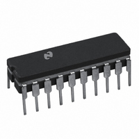
ADC1005BCJ-1 National Semiconductor, ADC1005BCJ-1 Datasheet - Page 4

ADC1005BCJ-1
Manufacturer Part Number
ADC1005BCJ-1
Description
IC ADC 10BIT MPU COMPAT 20-CDIP
Manufacturer
National Semiconductor
Datasheet
1.ADC1005BCJ-1.pdf
(16 pages)
Specifications of ADC1005BCJ-1
Number Of Bits
10
Data Interface
Parallel
Number Of Converters
1
Voltage Supply Source
Single Supply
Operating Temperature
-40°C ~ 85°C
Mounting Type
Through Hole
Package / Case
20-CDIP (0.300", 7.62mm)
Lead Free Status / RoHS Status
Contains lead / RoHS non-compliant
Other names
*ADC1005BCJ-1
Available stocks
Company
Part Number
Manufacturer
Quantity
Price
www.national.com
f
Clock Duty Cycle
t
t
Width
t
falling edge of RD to Output Data
Valid)
t
(Delay from Rising Edge of RD to
Hi-Z State)
t
WR or RD to Reset of INTR
t
Time
C
C
Outputs
CLK
C
W(WR)L
ACC
1H
WI
IRS
IN
OUT
, Conversion Time
AC Electrical Characteristics
The following specifications apply for V
apply from T
Note 1: Absolute Maximum Ratings indicate limits beyond which damage to the device may occur. DC and AC electrical specifications do not apply when operating
the device beyond its specified operating conditions.
Note 2: All voltages are measured with respect to ground.
Note 3: Linearity error is defined as the deviation of the analog value, expressed in LSBs, from the straight line which passes through the end points of the transfer
characteristic.
Note 4: For V
input voltages one diode drop below ground or one diode drop greater than V
inputs (5V) can cause this input diode to conduct, especially at elevated temperatures, and cause errors for analog inputs near full-scale. The spec allows 50 mV
forward bias of either diode. This means that as long as the analog V
To achieve an absolute 0 V
tolerance and loading.
Note 5: Typicals are at 25°C and represent most likely parametric norm.
Note 6: Tested and guaranteed to National's AOQL (Average Outgoing Quality Level).
Note 7: Guaranteed, but not 100% production tested. These limits are not used to calculate outgoing quality levels.
Note 8: Human body model, 100 pF discharged through a 1.5 kΩ resistor.
, t
, t
, Capacitance of Logic Inputs
, INTR to 1st Read Set-up
, Clock Frequency
, Access Time (Delay from
RI
0H
, Capacitance of Logic
, Delay from Falling Edge of
, TRI-STATE Control
, Minimum WR Pulse
Parameter
IN(−)
MIN
≥
V
IN(+)
to T
the digital output code will be 00 0000 0000. Two on-chip diodes are tied to each analog input which will forward conduct for analog
MAX
DC
MIN
MAX
MIN
MAX
MIN
MAX
MIN
MAX
to 5 V
; All other limits T
DC
input voltage range will therefore require a minimum supply voltage of 4.950 V
f
f
CS =0
CS =0
C
R
R
CLK
CLK
L
L
L
=100 pF, R
=10k, C
=2k, C
=1.8 MHz
=1.8 MHz
5261 Version 8 Revision 2
Conditions
CC
L
= 5V, V
=100 pF
L
A
=10 pF
= T
L
= 2k
j
= 25°C.
REF
= 5V,V
IN
does not exceed the supply voltage by more than 50 mV, the output code will be correct.
REF
Print Date/Time: 2009/08/26 22:47:16
(Note 5)
CC
4
= 5V, t
Typ
100
170
125
145
300
400
supply. Be careful, during testing at low V
5
5
r
= t
f
= 20 ns unless otherwise specified. Boldface limits
(Note 6)
Tested
Limit
150
300
230
450
550
0.2
2.6
40
60
80
90
45
50
DC
over temperature variations, initial
CC
levels (4.5V), as high level analog
(Note 7)
Design
Limit
150
300
200
230
450
550
0.2
2.6
7.5
7.5
40
60
80
90
45
50
Units
1/f
1/f
Limit
MHz
MHz
pF
pF
μs
μs
ns
ns
ns
ns
ns
ns
%
%
CLK
CLK


