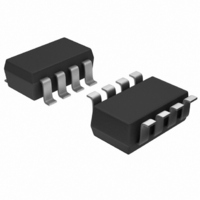
AD7453ART-REEL7 Analog Devices Inc, AD7453ART-REEL7 Datasheet - Page 18

AD7453ART-REEL7
Manufacturer Part Number
AD7453ART-REEL7
Description
IC ADC 12BIT DFF 600KSPS SOT23-8
Manufacturer
Analog Devices Inc
Datasheet
1.AD7453BRTZ-R2.pdf
(20 pages)
Specifications of AD7453ART-REEL7
Design Resources
Measuring -48 V High-Side Current Using AD629, AD8603, AD780, and AD7453 (CN0100)
Number Of Bits
12
Sampling Rate (per Second)
555k
Data Interface
DSP, MICROWIRE™, QSPI™, Serial, SPI™
Number Of Converters
1
Power Dissipation (max)
7.25mW
Voltage Supply Source
Single Supply
Operating Temperature
-40°C ~ 85°C
Mounting Type
Surface Mount
Package / Case
SOT-23-8
Lead Free Status / RoHS Status
Contains lead / RoHS non-compliant
AD7453
The timer registers, for example, are loaded with a value that
provides an interrupt at the required sample interval. When an
interrupt is received, a value is transmitted with TFS/DT (ADC
control word). The TFS is used to control the RFS and thus the
reading of data. The frequency of the serial clock is set in the
SCLKDIV register. When the instruction to transmit with TFS
is given, (i.e., AX0 = TX0), the state of the SCLK is checked. The
DSP waits until the SCLK has gone high, low, and high again
before transmission starts. If the timer and SCLK values are
chosen such that the instruction to transmit occurs on or near
the rising edge of SCLK, then the data may be transmitted or it
may wait until the next clock edge.
For example, the ADSP-2111 has a master clock frequency of
16 MHz. If the SCLKDIV register is loaded with the value 3, an
SCLK of 2 MHz is obtained and eight master clock periods
elapse for every SCLK period. If the timer registers are loaded
with the value 803, then 100.5 SCLKs occur between interrupts
and subsequently between transmit instructions. This situation
results in nonequidistant sampling as the transmit instruction is
occurring on an SCLK edge. If the number of SCLKs between
interrupts is a whole integer figure of N, equidistant sampling is
implemented by the DSP.
AD7453 to TMS320C5x/C54x
The serial interface on the TMS320C5x/C54x uses a continuous
serial clock and frame synchronization signals to synchronize
the data transfer operations with peripheral devices like the
AD7453. The CS input allows easy interfacing between the
TMS320C5x/C54x and the AD7453 without any glue logic
required. The serial port of the TMS320C5x/C54x is set up to
operate in burst mode with internal CLKx (Tx serial clock) and
FSx (Tx frame sync). The serial port control register (SPC) must
have the following setup: FO = 0, FSM = 1, MCM = 1 and TXM
= 1. The format bit, FO, may be set to 1 to set the word length to
eight bits in order to implement the power-down mode on the
AD7453. The connection diagram is shown in Figure 29. For
signal processing applications, it is imperative that the frame
synchronization signal from the TMS320C5x/C54x provide
equidistant sampling.
Rev. B | Page 18 of 20
AD7453 to DSP56xxx
The connection diagram in Figure 30 shows how the AD7453
can be connected to the SSI (synchronous serial interface) of
the DSP56xxx family of DSPs from Motorola. The SSI is
operated in synchronous mode (SYN bit in CRB = 1) with
internally generated 1-bit clock period frame sync for both Tx
and Rx (Bit FSL1 = 1 and Bit FSL0 = 0 in CRB). Set the word
length to 16 by setting Bits WL1 = 1 and WL0 = 0 in CRA. To
implement the power-down mode on the AD7453, the word
length can be changed to eight bits by setting Bits WL1 = 0 and
WL0 = 0 in CRA. For signal processing applications, it is
imperative that the frame synchronization signal from the
DSP56xxx provide equidistant sampling.
*ADDITIONAL PINS REMOVED FOR CLARITY
*ADDITIONAL PINS REMOVED FOR CLARITY
AD7453*
AD7453*
SDATA
SDATA
SCLK
SCLK
Figure 29. Interfacing to the TMS320C5x/C54x
CS
CS
Figure 30. Interfacing to the DSP56xxx
SCLK
SRD
SR2
CLKx
CLKR
DR
FSx
FSR
TMS320C5x/
DSP56xxx*
C54x*


