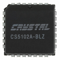
CS5102A-BLZ Cirrus Logic Inc, CS5102A-BLZ Datasheet - Page 25

CS5102A-BLZ
Manufacturer Part Number
CS5102A-BLZ
Description
IC ADC 16BIT 100/20KHZ 28-PLCC
Manufacturer
Cirrus Logic Inc
Datasheet
1.CS5101A-BL8Z.pdf
(39 pages)
Specifications of CS5102A-BLZ
Number Of Bits
16
Sampling Rate (per Second)
20k
Data Interface
Serial
Number Of Converters
1
Power Dissipation (max)
65mW
Voltage Supply Source
Analog and Digital, Dual ±
Operating Temperature
-40°C ~ 85°C
Mounting Type
Surface Mount
Package / Case
28-PLCC
Lead Free Status / RoHS Status
Lead free / RoHS Compliant
Other names
598-1079-5
Available stocks
Company
Part Number
Manufacturer
Quantity
Price
Company:
Part Number:
CS5102A-BLZ
Manufacturer:
Cirrus Logic Inc
Quantity:
10 000
Part Number:
CS5102A-BLZ
Manufacturer:
CRYSTAL
Quantity:
20 000
ry when the device is not sampling. It does not
require calibration after SLEEP is made inactive
(high). When coming out of Sleep mode, sampling
can begin as soon as the oscillator starts (time will
depend on the particular oscillator components)
and the REFBUF capacitor is charged (which
takes about 3 ms for the CS5101A, 50 ms for the
CS5102A). To achieve minimum start-up time, use
an external clock and leave the voltage reference
powered-up. Connect a resistor (2 kΩ) between
pins 20 and 21 to keep the REFBUF capacitor
charged. Conversion can then begin as soon as
the A/D circuitry has stabilized and performed a
track cycle.
To retain calibration memory while SLEEP is active
(low) VA+ and VD+ must be maintained at greater
than 2.0V. VA- and VD- can be allowed to go to 0
volts. The voltages into VA- and VD- cannot just be
“shut-off” as these pins cannot be allowed to float
to potentials greater than AGND/DGND. If the sup-
ply voltages to VA- and VD- are removed, use a
transistor switch to short these to the power supply
ground while in Sleep mode.
6.4
The CS5101A and CS5102A use the analog
ground connection, AGND, only as a reference
voltage. No DC power currents flow through the
AGND connection, and it is completely indepen-
dent of DGND. However, any noise riding on the
AGND input relative to the system's analog ground
will induce conversion errors. Therefore, both the
analog input and reference voltage should be re-
ferred to the AGND pin, which should be used as
the entire system's analog ground reference.
DS45F6
Grounding & Power Supply
Decoupling
The digital and analog supplies are isolated within
the CS5101A and CS5102A and are pinned out
separately to minimize coupling between the ana-
log and digital sections of the chip. All four supplies
should be decoupled to their respective grounds
using 0.1 µF ceramic capacitors. If significant low-
frequency noise is present on the supplies, tanta-
lum capacitors are recommended in parallel with
the 0.1 µF capacitors.
The positive digital power supply of the CS5101A
and CS5102A must never exceed the positive an-
alog supply by more than a diode drop or the
CS5101A and CS5102A could experience perma-
nent damage. If the two supplies are derived from
separate sources, care must be taken that the an-
alog supply comes up first at power-up. The sys-
tem connection diagram (Figure 9) shows a
decoupling scheme which allows the CS5101A
and CS5102A to be powered from a single set of
5V rails. The positive digital supply is derived from
the analog supply through a 10 Ω resistor to avoid
the analog supply dropping below the digital sup-
ply. If this scheme is utilized, care must be taken to
ensure that any digital load currents (which flow
through the 10 Ω resistors) do not cause the mag-
nitude of digital supplies to drop below the analog
supplies by more than 0.5 volts. Digital supplies
must always remain above the minimum specifica-
tion.
As with any high-precision A/D converter, the
CS5101A and CS5102A require careful attention
to grounding and layout arrangements. However,
no unique layout issues must be addressed to
properly apply the devices.
CS5101A CS5102A
25


