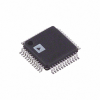
AD7667AST Analog Devices Inc, AD7667AST Datasheet - Page 5

AD7667AST
Manufacturer Part Number
AD7667AST
Description
IC ADC 16BIT UNIPOLAR 48-LQFP
Manufacturer
Analog Devices Inc
Series
PulSAR®r
Datasheet
1.AD7667ASTZ.pdf
(28 pages)
Specifications of AD7667AST
Rohs Status
RoHS non-compliant
Number Of Bits
16
Sampling Rate (per Second)
1M
Data Interface
Serial, Parallel
Number Of Converters
1
Power Dissipation (max)
145mW
Voltage Supply Source
Analog and Digital
Operating Temperature
-40°C ~ 85°C
Mounting Type
Surface Mount
Package / Case
48-LQFP
For Use With
EVAL-AD7667CBZ - BOARD EVALUATION FOR AD7667
Available stocks
Company
Part Number
Manufacturer
Quantity
Price
Company:
Part Number:
AD7667AST
Manufacturer:
ADI
Quantity:
329
Company:
Part Number:
AD7667ASTZ
Manufacturer:
ADI
Quantity:
306
Company:
Part Number:
AD7667ASTZ
Manufacturer:
Analog Devices Inc
Quantity:
10 000
Part Number:
AD7667ASTZ
Manufacturer:
ADI/亚德诺
Quantity:
20 000
Company:
Part Number:
AD7667ASTZRL
Manufacturer:
Analog Devices Inc
Quantity:
10 000
TIMING SPECIFICATIONS
Table 3. –40°C to +85°C, AVDD = DVDD = 5 V, OVDD = 2.7 V to 5.25 V, unless otherwise noted.
Parameter
Refer to Figure 33 and Figure 34
Refer to Figure 35, Figure 36, and Figure 37 (Parallel Interface Modes)
Refer to Figure 39 and Figure 40 (Master Serial Interface Modes)
Refer to Figure 41 and Figure 42 (Slave Serial Interface Modes)
1
2
3
In Warp mode only, the time between conversions is 1ms; otherwise there is no required maximum time.
In serial interface modes, the SYNC, SCLK, and SDOUT timings are defined with a maximum load C
In Serial Master Read During Convert mode. See Table 4 for Serial Master Read After Convert Mode.
Convert Pulse Width
Time between Conversions (Warp Mode/Normal Mode/Impulse Mode)
CNVST LOW to BUSY HIGH Delay
BUSY HIGH All Modes except Master Serial Read after Convert
Aperture Delay
End of Conversion to BUSY LOW Delay
Conversion Time
Acquisition Time
RESET Pulse Width
CNVST LOW to DATA Valid Delay
DATA Valid to BUSY LOW Delay
Bus Access Request to DATA Valid
Bus Relinquish Time
CS LOW to SYNC Valid Delay
CS LOW to Internal SCLK Valid Delay
CS LOW to SDOUT Delay
CNVST LOW to SYNC Delay
SYNC Asserted to SCLK First Edge Delay
Internal SCLK Period
Internal SCLK HIGH
Internal SCLK LOW
SDOUT Valid Setup Time
SDOUT Valid Hold Time
SCLK Last Edge to SYNC Delay
CS HIGH to SYNC HI-Z
CS HIGH to Internal SCLK HI-Z
CS HIGH to SDOUT HI-Z
BUSY HIGH in Master Serial Read after Convert
CNVST LOW to SYNC Asserted Delay
SYNC Deasserted to BUSY LOW Delay
External SCLK Setup Time
External SCLK Active Edge to SDOUT Delay
SDIN Setup Time
SDIN Hold Time
External SCLK Period
External SCLK HIGH
External SCLK LOW
3
3
3
3
3
3
2
3
Rev. 0 | Page 5 of 28
2
2
1
t
L
Symbol
t
t
t
t
t
t
t
t
t
t
t
t
t
t
t
t
t
t
t
t
t
t
t
t
t
t
t
t
t
t
t
t
t
t
t
t
1
2
3
4
5
6
7
8
9
10
11
12
13
14
15
16
17
18
19
20
21
22
23
24
25
26
27
28
29
30
31
32
33
34
35
36
37
of 10 pF; otherwise, the load is 60 pF maximum.
Min
10
1/1.25/1.5
10
250
10
12
5
3
25
12
7
4
2
3
5
3
5
5
25
10
10
Typ
2
25/275/525
See Table 4
0.75/1/1.25
25
Max
35
0.75/1/1.25
0.75/1/1.25
0.75/1/1.25
45
15
10
10
10
40
10
10
10
18
AD7667
Unit
ns
µs
ns
µs
ns
ns
µs
ns
ns
µs
ns
ns
ns
ns
ns
ns
ns
ns
ns
ns
ns
ns
ns
ns
ns
ns
ns
µs
ns
ns
ns
ns
ns
ns
ns
ns


