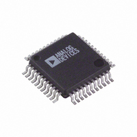
AD9260ASRL Analog Devices Inc, AD9260ASRL Datasheet - Page 9

AD9260ASRL
Manufacturer Part Number
AD9260ASRL
Description
IC ADC 16BIT 2.5MHZ 44-MQFP T/R
Manufacturer
Analog Devices Inc
Datasheet
1.AD9260ASZRL.pdf
(44 pages)
Specifications of AD9260ASRL
Rohs Status
RoHS non-compliant
Number Of Bits
16
Sampling Rate (per Second)
20M
Data Interface
Parallel
Number Of Converters
1
Power Dissipation (max)
585mW
Voltage Supply Source
Analog and Digital
Operating Temperature
-40°C ~ 85°C
Mounting Type
Surface Mount
Package / Case
44-MQFP, 44-PQFP
DIGITAL SPECIFICATIONS
AVDD = +5 V, DVDD = +5 V, T
Table 8.
Parameter
CLOCK
LOGIC OUTPUTS (with DRVDD = 5 V)
LOGIC OUTPUTS (with DRVDD = 3 V)
1
2
Since CLK is referenced to AVDD, +5 V logic input levels only apply.
The AD9260 is not guaranteed to meet V
High Level Input Voltage
Low Level Input Voltage
High Level Input Current (V
Low Level Input Current (V
Input Capacitance
High Level Output Voltage (I
High Level Output Voltage (I
Low Level Output Voltage
Low Level Output Voltage (I
Output Capacitance
High Level Output Voltage (I
Low Level Output Voltage (I
(DVDD = +5 V)
(DVDD = +3 V)
(DVDD = +5 V)
(DVDD = +3 V)
1
AND LOGIC INPUTS
ANALOG INPUT
DATA OUTPUT
INPUT CLOCK
READ
DAV
CS
2
IN
IN
(I
OL
OL
= 0 V)
OH
OH
OH
OL
t
= DVDD)
H
= 50 µA)
= 50 µA)
S1
MIN
= 0.3 mA)
= 50 µA)
= 0.5 mA)
= 50 µA)
t
CH
OL
to T
t
= 0.4 V max for standard TTL load of I
C
t
CL
S2
MAX
t
DI
unless otherwise noted.
AD9260
+3.5
+2.1
+1.0
+0.9
± 10
± 10
5
+4.5
+2.4
+0.4
+0.1
5
+2.4
+0.7
Figure 8. Timing Diagram
Rev. C | Page 9 of 44
t
t
DAV
OL
DS
= 1.6 mA.
Unit
V min
V max
V min
V max
µA max
µA max
pF typ
V min
V min
V max
V max
pF typ
V min
V max
t
OD
t
OE
AD9260


