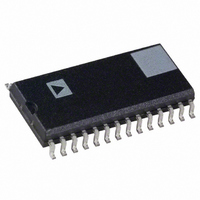
AD9066JR-REEL Analog Devices Inc, AD9066JR-REEL Datasheet - Page 4

AD9066JR-REEL
Manufacturer Part Number
AD9066JR-REEL
Description
IC ADC 6BIT DUAL 60MSPS 28-SOIC
Manufacturer
Analog Devices Inc
Datasheet
1.AD9066ARS.pdf
(7 pages)
Specifications of AD9066JR-REEL
Rohs Status
RoHS non-compliant
Number Of Bits
6
Sampling Rate (per Second)
60M
Data Interface
Parallel
Number Of Converters
2
Power Dissipation (max)
600mW
Voltage Supply Source
Analog and Digital
Operating Temperature
0°C ~ 70°C
Mounting Type
Surface Mount
Package / Case
28-SOIC (0.300", 7.50mm Width)
USING THE AD9066
Analog Input and Voltage References
The AD9066 is optimized to allow ac coupled inputs with a full-
scale input range of 500 mV ± 5%. An LSB weight is approxi-
mately 8 mV. The full-scale input range is defined as the voltage
range that accommodates 2
(between the first and last code transitions). For the AD9066
there are 32 codes above and below the midscale voltage of the
A see Figure 3).
The full-scale input range of the AD9066 is equal to 500/620 ×
(VT – VB), or nominally 500 mV. For dc coupled applications,
the REF A and REF B voltages can be used to feed back offset
compensation signals. This will allow the midscale transition
voltage of the ADCs to track supply and temperature variations.
In the event that offset correction signals are generated digitally,
the REF pins would not be required. Figure 4a shows the
equivalent circuit for the internal references. All component
tolerances are ± 25%.
AD9066
5.8
5.7
5.6
5.5
5.4
5.3
5.2
5.8
5.7
5.6
5.5
5.4
5.3
5.2
10
1
n
– 2 codes of equally weighted LSBs
MHz
MHz
10
ANALOG INPUT = 10.1MHz
ENCODE = 60MSPS
100
100
Gain Variation
The full-scale input range is established by the current through
the two matched resistor ladders (620 ohms each nominal). There-
fore the gain of the ADC may be modified by forcing different
voltages across the top and bottom voltage taps (VT and VB).
The easiest way to increase the input range will be to force VB
to a lower voltage. Using an external amplifier, the voltage at VB
may be forced as low as 3.0 V (3.58 nominal). Using the pre-
viously described relationship for full scale and the internal
resistor ladder values, 3.0 V at VB will result in a nominal full-
scale input range of 705 mV.
A larger input range can be established by taking the VT voltage
all the way to the supply voltage level while pulling VB to 3.0 V.
This would force a 2 V potential across the ladder and create a
full-scale input range of 1.6 V.
Greater flexibility and improved power supply rejection can be
achieved by forcing external voltage references at both the top
and bottom of the resistor ladder.
REF B
VB
VT
–FULL-SCALE
40k
000000
310
310
+V
000001
S
V
= 5V
310
310
S
400
2mA
OUTPUTS
40k
100000
2
n
MIDSCALE
–2 = 62
REF A
011111
INPUT
111111
+FULL-SCALE
40k
REF
1.4V THRESHOLD
V
S
V
S


