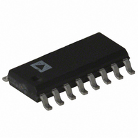
AD7888AR Analog Devices Inc, AD7888AR Datasheet - Page 7

AD7888AR
Manufacturer Part Number
AD7888AR
Description
IC ADC 12BIT 8CH SRL 16-SOIC
Manufacturer
Analog Devices Inc
Datasheet
1.AD7888ARZ.pdf
(17 pages)
Specifications of AD7888AR
Rohs Status
RoHS non-compliant
Number Of Bits
12
Sampling Rate (per Second)
125k
Data Interface
DSP, MICROWIRE™, QSPI™, Serial, SPI™
Number Of Converters
1
Power Dissipation (max)
3.5mW
Voltage Supply Source
Single Supply
Operating Temperature
-40°C ~ 105°C
Mounting Type
Surface Mount
Package / Case
16-SOIC (0.154", 3.90mm Width)
Available stocks
Company
Part Number
Manufacturer
Quantity
Price
Company:
Part Number:
AD7888AR
Manufacturer:
JOHANSON
Quantity:
15 000
Part Number:
AD7888AR
Manufacturer:
ADI/亚德诺
Quantity:
20 000
Part Number:
AD7888AR.
Manufacturer:
ADI/亚德诺
Quantity:
20 000
Part Number:
AD7888ARU
Manufacturer:
ADI/亚德诺
Quantity:
20 000
Part Number:
AD7888ARU-REEL7
Manufacturer:
ADI/亚德诺
Quantity:
20 000
Company:
Part Number:
AD7888ARUZ
Manufacturer:
ADI
Quantity:
1 000
Part Number:
AD7888ARUZ
Manufacturer:
ADI/亚德诺
Quantity:
20 000
REV. C
PERFORMANCE CURVES
Figure 2 shows a typical FFT plot for the AD7888 at 100 kHz
sample rate and 10 kHz input frequency.
CONTROL REGISTER
The Control Register on the AD7888 is an 8-bit, write-only register. Data is loaded from the DIN pin of the AD7888 on the rising
edge of SCLK. The data is transferred on the DIN line at the same time as the conversion result is read from the part. This requires
16 serial clocks for every data transfer. Only the information provided on the first 8 rising clock edges (after CS falling edge) is loaded
to the Control Register. MSB denotes the first bit in the data stream. The bit functions are outlined in Table I. The default contents
of the Control Register on power-up is all zeros.
Bit
7
6
5
4
3
2
1, 0
–110
Mnemonic
DONTC
ZERO
ADD2
ADD1
ADD0
REF
PM1, PM0
–10
–30
–50
–70
–90
0
MSB
D
12.21
O
Comment
Don’t Care. The value written to this bit of the Control Register is a don’t care, i.e., it doesn’t matter if the bit is
0 or 1.
A zero must be written to this bit to ensure correct operation of the AD7888.
These three address bits are loaded at the end of the present conversion sequence and select which analog input
channel is converted for the next conversion. The selected input channel is decoded as shown in Table II.
Reference Bit. With a 0 in this bit, the on-chip reference is enabled. With a 1 in this bit, the on-chip reference
is disabled. To obtain best performance from the AD7888, the internal reference should be disabled when
using an externally applied reference source. (See On-Chip Reference section.)
Power Management Bits. These two bits decode the mode of operation of the AD7888 as shown in Table III.
N
T
FREQUENCY – kHz
C
24.41
Z
E
R
O
Table I. Control Register Bit Function Description
4096 POINT FFT
SAMPLING
100kSPS
f
SNR = 70dB
IN
= 10kHz
36.62
A
D
D
2
48.83
A
D
D
1
Figure 3 shows a typical plot for the SNR vs. frequency for a
5 V supply and with a 5 V external reference.
A
D
D
0
73.0
72.5
72.0
71.5
71.0
0
R
E
F
10.89
INPUT FREQUENCY – kHz
P
M
1
21.14
P
V
5V EXT REFERENCE
DD
M
= 5V
0
31.59
AD7888
42.14


