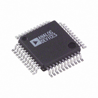
AD7865BS-1 Analog Devices Inc, AD7865BS-1 Datasheet - Page 11

AD7865BS-1
Manufacturer Part Number
AD7865BS-1
Description
IC ADC 14BIT 4CH 5V 44-MQFP
Manufacturer
Analog Devices Inc
Specifications of AD7865BS-1
Rohs Status
RoHS non-compliant
Number Of Bits
14
Sampling Rate (per Second)
350k
Data Interface
Parallel
Number Of Converters
1
Power Dissipation (max)
160mW
Voltage Supply Source
Analog and Digital
Operating Temperature
-40°C ~ 85°C
Mounting Type
Surface Mount
Package / Case
44-MQFP, 44-PQFP
Available stocks
Company
Part Number
Manufacturer
Quantity
Price
Company:
Part Number:
AD7865BS-1
Manufacturer:
ADI
Quantity:
329
AD7865-3
Figure 4 shows the analog input section of the AD7865-3. The
analog input range is 2.5 V on the V
input can be left unconnected but if it is connected to a poten-
tial then that potential must be AGND.
For the AD7865-3, R1 = 4 k and R2 = 4 k
V
resistor input stage is followed by the high input impedance
stage of the track/hold amplifier.
The designed code transitions take place midway between suc-
cessive integer LSB values (i.e., 1/2 LSB, 3/2 LSBs, 5/2 LSBs
etc.) LSB size is given by the formula, 1 LSB = FSR/16384.
Output coding is twos complement binary with 1 LSB = FSR/
16384 = 5 V/16384 = 610.4 V. The ideal input/output transfer
function for the AD7865-3 is shown in Table III.
Analog Input
+FSR/2 – 3/2 LSB
+FSR/2 – 5/2 LSB
+FSR/2 – 7/2 LSB
AGND + 3/2 LSB
AGND + 1/2 LSB
AGND – 1/2 LSB
AGND – 3/2 LSB
–FSR/2 + 5/2 LSB
–FSR/2 + 3/2 LSB
–FSR/2 + 1/2 LSB
NOTES
1
2
SELECTING A CONVERSION SEQUENCE
Any subset of the four channels V
conversion. The selected channels are converted in an ascending
order. For example if the channel selection includes V
and V
then V
using either the hardware channel select input pins SL1 through
SL4 (if H/S is tied low) or programming the channel select
register (if H/S is tied high). A logic high on a hardware channel
select pin (or logic one in the channel select register) when
CONVST goes logic high, marks the associated analog input
channel for inclusion in the conversion sequence.
REV. A
FSR is full-scale range is 5 V, with V
1 LSB = FSR/16384 = 610.4 V ( 2.5 V—AD7865-3) with V
INxA
Table III. Ideal Input/Output Code Table for the AD7865-3
V
V
input should be driven from a low impedance source. The
IN3
V
IN4
INxA
INxB
REF
Figure 4. AD7865-3 Analog Input Structure
then the conversion sequence will be V
. The conversion sequence selection may be made by
6k
1
2
R2
REFERENCE
R1
011 . . . 101 to 011 . . . 110
011 . . . 100 to 011 . . . 101
111 . . . 111 to 000 . . . 000
111 . . . 110 to 111 . . . 111
100 . . . 010 to 100 . . . 011
100 . . . 001 to 100 . . . 010
100 . . . 000 to 100 . . . 001
Digital Output Code Transition
011 . . . 110 to 011 . . . 111
000 . . . 001 to 000 . . . 010
000 . . . 000 to 000 . . . 001
+2.5V
REF
= +2.5 V.
IN1
TO ADC
REFERENCE
CIRCUITRY
TRACK/
HOLD
to V
INxA
IN4
AD7865-3
input. The V
can be selected for
TO INTERNAL
COMPARATOR
As a result, the
IN1
REF
, V
= +2.5 V.
IN4
IN3
, V
and
INxB
IN1
–11–
Figure 5 shows the arrangement used. The H/S SEL controls a
multiplexer that selects the source of the conversion sequence
information, i.e., from the hardware channel select pins (SL1 to
SL4) or from the channel selection register. When a conversion
is started the output from the multiplexer is latched until the
end-of-the conversion sequence. The data bus bits DB0 to DB3
(DB0 representing Channel 1 through DB3 representing Chan-
nel 4) are bidirectional and become inputs to the channel select
register when RD is logic high and CS and WR are logic low.
The logic state on DB0 to DB3 is latched into the channel select
register when WR goes logic high. Figure 6 shows the loading
sequence for channel selection using software control. When
using software control to select the conversion sequence a write
is only required each time the conversion sequence needs chang-
ing. This is because the channel select register will hold its in-
formation until different information is written to it.
It should be noted that the hardware select Pins SL1 and SL2
are dual function. When H/S SEL is logic low (selecting the
conversion sequence using software control) they take the func-
tions CLK IN and INT/EXT CLK respectively. Therefore, the
logic inputs on these pins must be set according to the type of
operation required (see Using an External Clock). Also when
H/S SEL is high, the SL3 and SL4 logic inputs have no function
and can be tied either high or low, but should not be left floating.
WR
CS
D3
DATA BUS
Figure 6. Channel Selection via Software Control
D2
Figure 5. Channel Select Inputs and Registers
HARDWARE CHANNEL
D1
DATA
WR
SELECT PINS
RD
CS
D0
REGISTER
CHANNEL
SELECT
WR
SL3
SL4
SL1
SL2
TRANSPARENT WHILE WAITING FOR CONVST.
LATCHED ON THE RISING EDGE OF CONVST AND
DURING A CONVERSION SEQUENCE.
t
14
MULTIPLEXER
t
t
H/S
16
13
DATA IN
t
15
t
17
LATCH
AD7865
SELECT INDIVIDUAL
TRACK-AND-HOLDS
FOR CONVERSION
SEQUENCER


