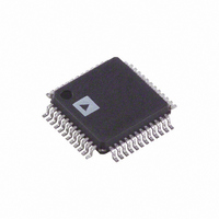
AD7660AST Analog Devices Inc, AD7660AST Datasheet - Page 15

AD7660AST
Manufacturer Part Number
AD7660AST
Description
IC ADC 16BIT UNIPOLAR 48-LQFP
Manufacturer
Analog Devices Inc
Series
PulSAR®r
Datasheet
1.AD7660ASTZRL.pdf
(20 pages)
Specifications of AD7660AST
Rohs Status
RoHS non-compliant
Number Of Bits
16
Sampling Rate (per Second)
100k
Data Interface
Serial, Parallel
Number Of Converters
1
Power Dissipation (max)
25mW
Voltage Supply Source
Analog and Digital
Operating Temperature
-40°C ~ 85°C
Mounting Type
Surface Mount
Package / Case
48-LQFP
For Use With
EVAL-AD7660CBZ - BOARD EVALUATION FOR AD7660
Available stocks
Company
Part Number
Manufacturer
Quantity
Price
Company:
Part Number:
AD7660AST
Manufacturer:
BROADCOM
Quantity:
27
Company:
Part Number:
AD7660AST
Manufacturer:
ADI
Quantity:
300
Company:
Part Number:
AD7660ASTZ
Manufacturer:
ATMEL
Quantity:
36
Company:
Part Number:
AD7660ASTZ
Manufacturer:
ADI
Quantity:
246
Company:
Part Number:
AD7660ASTZ
Manufacturer:
Analog Devices Inc
Quantity:
10 000
Part Number:
AD7660ASTZ
Manufacturer:
ADI/亚德诺
Quantity:
20 000
Company:
Part Number:
AD7660ASTZRL
Manufacturer:
Analog Devices Inc
Quantity:
10 000
REV. D
DATA BUS
CNVST,
CS = 0
BUSY
Figure 15. Slave Parallel Data Timing for Reading
(Read during Convert)
RD
SDOUT
CNVST
SDOUT
CS, RD
CNVST
CS, RD
BUSY
SYNC
SCLK
BUSY
SYNC
SCLK
t
Figure 17. Master Serial Data Timing for Reading (Read Previous Conversion during Convert)
12
t
3
CONVERSION
t
16
PREVIOUS
t
1
Figure 16. Master Serial Data Timing for Reading (Read after Convert)
t
t
3
13
t
t
t
14
15
16
t
t
t
14
15
29
t
17
X
t
t
18
22
t
4
EXT/INT = 0
t
EXT/INT = 0
1
t
D15
3
X
t
t
1
20
22
t
19
t
21
t
20
D14
t
D15
2
23
1
t
t
19
18
RDC/SDIN = 0
RDC/SDIN = 1
D14
t
2
t
21
3
23
–15–
t
28
SERIAL INTERFACE
The AD7660 is configured to use the serial interface when the
SER/PAR is held HIGH. The AD7660 outputs 16 bits of data,
MSB first, on the SDOUT pin. This data is synchronized with
the 16 clock pulses provided on the SCLK pin.
MASTER SERIAL INTERFACE
Internal Clock
The AD7660 is configured to generate and provide the serial data
clock SCLK when the EXT/INT pin is held LOW. The AD7660
also generates a SYNC signal to indicate to the host when the
serial data is valid. The serial clock SCLK and the SYNC signal
can be inverted if desired. The output data is valid on both the
rising and falling edge of the data clock. Depending on RDC/
SDIN input, the data can be read after each conversion or during
the following conversion. Figures 16 and 17 show the detailed timing
diagrams of these two modes.
3
INVSCLK = INVSYNC = 0
14
D2
INVSCLK = INVSYNC = 0
14
D2
15
D1
15
D1
16
t
24
16
t
30
D0
t
D0
24
t
t
t
t
t
t
26
25
27
25
26
27
AD7660


