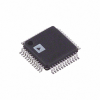
AD9244BST-65 Analog Devices Inc, AD9244BST-65 Datasheet - Page 18

AD9244BST-65
Manufacturer Part Number
AD9244BST-65
Description
IC ADC 14BIT 65MSPS 48-LQFP
Manufacturer
Analog Devices Inc
Datasheet
1.AD9244BSTZ-65.pdf
(36 pages)
Specifications of AD9244BST-65
Rohs Status
RoHS non-compliant
Number Of Bits
14
Sampling Rate (per Second)
65M
Data Interface
Parallel
Number Of Converters
1
Power Dissipation (max)
550mW
Voltage Supply Source
Analog and Digital
Operating Temperature
-40°C ~ 85°C
Mounting Type
Surface Mount
Package / Case
48-LQFP
For Use With
AD9244-65PCBZ - BOARD EVAL FOR AD9244-65AD9244-40PCBZ - BOARD EVAL FOR AD9244-40
Available stocks
Company
Part Number
Manufacturer
Quantity
Price
Company:
Part Number:
AD9244BST-65
Manufacturer:
ADI
Quantity:
624
Part Number:
AD9244BST-65
Manufacturer:
ADI/亚德诺
Quantity:
20 000
AD9244
A differential input structure allows the user to easily configure the
inputs for either single-ended or differential operation. The ADC’s
input structure allows the dc offset of the input signal to be varied
independent of the input span of the converter. Specifically, the
input to the ADC core can be defined as the difference of the
voltages applied at the VIN+ and VIN– input pins.
Therefore, the equation
defines the output of the differential input stage and provides
the input to the ADC core. The voltage, V
condition
where VREF is the voltage at the VREF pin.
In addition to the limitations placed on the input voltages VIN+
and VIN– by Equation 1 and Equation 2, boundaries on the
inputs also exist based on the power supply voltages according
to the conditions
where:
AGND is nominally 0 V.
AVDD is nominally 5 V.
Table 8. Analog Input Configuration Summary
Input
Connection
Single-Ended
Differential
1
Table 9. Reference Configuration Summary
Reference Operating Mode
Internal
Internal
Internal
External
VIN+ and VIN− can be interchanged if data inversion is required.
V
−VREF/2 < V
AGND − 0.3 V < VIN+ < AVDD + 0.3 V
AGND − 0.3 V < VIN− < AVDD + 0.3 V
CORE
= (VIN+) – (VIN−)
Coupling
DC or AC
DC or AC
CORE
< VREF/2
Input
Span (V)
1.0
2.0
1.0
2.0
Connect
SENSE
SENSE
R1
R2
SENSE
VREF
CORE
Input Range (V)
VIN+
0.5 to 1.5
1 to 3
2.25 to 2.75
2.0 to 3.0
, must satisfy the
1
To
AGND
SENSE and REFGND
AVDD
EXTERNAL REF
VREF
VREF and SENSE
VIN−
1.0
2.0
2.75 to 2.25
3.0 to 2.0
Rev. C | Page 18 of 36
(1)
(2)
(3)
(4)
1
Input CM
Voltage (V)
1.0
2.0
2.5
2.5
The range of valid inputs for VIN+ and VIN− is any combination
that satisfies Equation 2, Equation 3, and Equation 4.
For additional information showing the relationship between
VIN+, VIN–, VREF, and the analog input range of the AD9244,
see Table 8 and Table 9.
ANALOG INPUT OPERATION
Figure 44 shows the equivalent analog input of the AD9244,
which consists of a 750 MHz differential SHA. The differential
input structure of the SHA is flexible, allowing the device to be
configured for either a differential or single-ended input. The
analog inputs VIN+ and VIN– are interchangeable, with the
exception that reversing the inputs to the VIN+ and VIN– pins
results in a data inversion (complementing the output word).
Resulting VREF (V)
1
2
1 ≤ VREF ≤ 2.0
VREF = (1 + R1/R2)
1 ≤ VREF ≤ 2.0
VIN+
VIN–
C
C
PIN, PAR
PIN, PAR
Comments
Best for stepped input response applications.
Optimum noise performance for single-ended
mode often requires low distortion op amp
with VCC > 5 V due to its headroom issues.
Optimum full-scale THD and SFDR performance
well beyond the ADC’s Nyquist frequency.
Optimum noise performance for differential
mode. Preferred mode for applications.
Figure 44. Analog Input of AD9244 SHA
S
S
H
Input Span (VIN+ − VIN−) (V p-p)
1
2
1 ≤ SPAN ≤ 2
(SPAN = VREF)
SPAN = EXTERNAL REF
C
C
S
S
C
C
S
S
H
H


