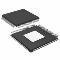
AD9430BSV-210 Analog Devices Inc, AD9430BSV-210 Datasheet - Page 11

AD9430BSV-210
Manufacturer Part Number
AD9430BSV-210
Description
IC ADC 12BIT 210MSPS 3.3V100TQFP
Manufacturer
Analog Devices Inc
Datasheet
1.AD9430BSVZ-210.pdf
(44 pages)
Specifications of AD9430BSV-210
Rohs Status
RoHS non-compliant
Number Of Bits
12
Sampling Rate (per Second)
210M
Data Interface
Parallel
Number Of Converters
1
Power Dissipation (max)
1.7mW
Voltage Supply Source
Single Supply
Operating Temperature
-40°C ~ 85°C
Mounting Type
Surface Mount
Package / Case
100-TQFP Exposed Pad
Number Of Elements
1
Resolution
12Bit
Architecture
Pipelined
Sample Rate
210MSPS
Input Polarity
Unipolar
Input Type
Voltage
Rated Input Volt
0.766/1.536V
Differential Input
Yes
Power Supply Requirement
Single
Single Supply Voltage (typ)
3.3V
Single Supply Voltage (min)
3.2V
Single Supply Voltage (max)
3.6V
Dual Supply Voltage (typ)
Not RequiredV
Dual Supply Voltage (min)
Not RequiredV
Dual Supply Voltage (max)
Not RequiredV
Power Dissipation
1.7W
Differential Linearity Error
±1.75LSB
Integral Nonlinearity Error
±2.5LSB
Operating Temp Range
-40C to 85C
Operating Temperature Classification
Industrial
Mounting
Surface Mount
Pin Count
100
Package Type
TQFP EP
Input Signal Type
Differential
Lead Free Status / RoHS Status
Not Compliant
Available stocks
Company
Part Number
Manufacturer
Quantity
Price
Company:
Part Number:
AD9430BSV-210
Manufacturer:
AD
Quantity:
1 831
Company:
Part Number:
AD9430BSV-210
Manufacturer:
AD
Quantity:
648
PIN CONFIGURATIONS AND FUNCTION DESCRIPTIONS
Table 7. CMOS Mode Pin Function Descriptions
Pin Number
1
2, 7, 42, 43, 65, 66, 68
3
4, 9, 12, 13, 16, 17, 20, 23, 25, 26, 30, 31, 35, 38, 41, 86,
87, 91, 92, 93, 96, 97, 100
5
6
8, 14, 15, 18, 19, 24, 27, 28, 29, 34, 39, 40, 88, 89, 90, 94,
95, 98, 99
10
11
21
22
32
33
SENSE
NOTES
AGND
AGND
AGND
AGND
AGND
AGND
AGND
AGND
AGND
AVDD
AVDD
AVDD
AVDD
AVDD
AVDD
1. THE AD9430 HAS A CONDUCTIVE HEAT SLUG TO HELP DISSIPATE HEAT AND ENSURE RELIABLE OPERATION OF
VREF
VIN+
DNC
DNC
VIN–
THE DEVICE OVER THE FULL INDUSTRIAL TEMPERATURE RANGE. THE SLUG IS EXPOSED ON THE BOTTOM OF
THE PACKAGE AND ELECTRICALLY CONNECTED TO CHIP GROUND. IT IS RECOMMENDED THAT NO PCB SIGNAL
TRACES OR VIAS BE LOCATED UNDER THE PACKAGE THAT COULD COME IN CONTACT WITH THE CONDUCTIVE
SLUG. ATTACHING THE SLUG TO A GROUND PLANE WILL REDUCE THE JUNCTION TEMPERATURE OF THE
DEVICE WHICH MAY BE BENEFICIAL IN HIGH TEMPERATURE ENVIRONMENTS.
S5
S4
S2
S1
10
11
12
13
14
15
16
17
18
19
20
21
22
23
24
25
1
2
3
4
5
6
7
8
9
26 27 28 29 30 31 32 33 34 35 36 37 38 39 40 41 42 43 44 45 46 47 48 49 50
100
PIN 1
99
98
97
96
95
Figure 4. CMOS Dual-Mode Pin Configuration
94
93
92
Mnemonic
S5
DNC
S4
AGND
S2
S1
AVDD
SENSE
VREF
VIN+
VIN–
DS+
DS–
91
Rev. E | Page 11 of 44
CMOS PINOUT
90
(Not to Scale)
2
AD9430
TOP VIEW
89
1
88
87
86
Description
Full-Scale Adjust Pin. AVDD sets f
GND sets f
Do Not Connect.
Interleaved, Parallel Select Pin. High = interleaved.
Analog Ground.
Output Mode Select. Low = dual-port CMOS, high = LVDS.
Data Format Select. Low = binary, high = twos complement for
both CMOS and LVDS modes.
3.3 V Analog Supply.
Reference Mode Select Pin. Float for internal reference operation.
1.235 V Reference I/O—Function Dependent on SENSE.
Analog Input—True.
Analog Input—Complement.
Data Sync (Input)—True. Tie low if not used.
Data Sync (Input)—Complement. Tie high if not used.
85
84
83
S
82
= 1.536 V p-p differential.
81
80
79
78
77
76
75
74
73
72
71
70
69
68
67
66
65
64
62
61
60
58
57
56
54
53
52
63
59
55
51
S
= 0.768 V p-p differential,
DRVDD
DRGND
DA4
DA3
DA2
DA1
DA0
DNC
DRGND
DNC
DNC
DCO+
DCO–
DRVDD
DRGND
OR_B
DB11
DB10
DB9
DB8
DB7
DRVDD
DRGND
DB6
DB5
AD9430


