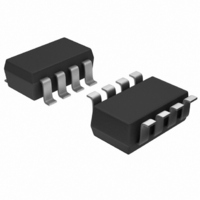
AD7453BRT-R2 Analog Devices Inc, AD7453BRT-R2 Datasheet - Page 19

AD7453BRT-R2
Manufacturer Part Number
AD7453BRT-R2
Description
IC ADC 12BIT 555KSPS SOT23-8
Manufacturer
Analog Devices Inc
Datasheet
1.AD7453BRTZ-R2.pdf
(20 pages)
Specifications of AD7453BRT-R2
Rohs Status
RoHS non-compliant
Design Resources
Measuring -48 V High-Side Current Using AD629, AD8603, AD780, and AD7453 (CN0100)
Number Of Bits
12
Sampling Rate (per Second)
555k
Data Interface
DSP, MICROWIRE™, QSPI™, Serial, SPI™
Number Of Converters
1
Power Dissipation (max)
7.25mW
Voltage Supply Source
Single Supply
Operating Temperature
-40°C ~ 85°C
Mounting Type
Surface Mount
Package / Case
SOT-23-8
Other names
AD7453BRT-R2TR
APPLICATION HINTS
Grounding and Layout
The printed circuit board that houses the AD7453 should be
designed so that the analog and digital sections are separated
and confined to certain areas of the board. This facilitates the
use of ground planes that can be easily separated. A minimum
etch technique is generally best for ground planes as it gives the
best shielding. Digital and analog ground planes should be
joined in only one place, and the connection should be a star
ground point established as close to the GND pin on the
AD7453 as possible.
Avoid running digital lines under the device as this couples
noise onto the die. The analog ground plane should be allowed
to run under the AD7453 to avoid noise coupling. The power
supply lines to the AD7453 should use as large a trace as
possible to provide low impedance paths and reduce the effects
of glitches on the power supply line.
Fast switching signals like clocks should be shielded with digital
ground to avoid radiating noise to other sections of the board,
and clock signals should never run near the analog inputs.
Avoid crossover of digital and analog signals. Traces on opposite
sides of the board should run at right angles to each other. This
reduces the effects of feedthrough through the board. A
microstrip technique is by far the best but is not always possible
with a double-sided board.
Rev. B | Page 19 of 20
In this technique, the component side of the board is dedicated
to ground planes while signals are placed on the solder side.
Good decoupling is also important. All analog supplies should
be decoupled with 10 µF tantalum capacitors in parallel with
0.1 µF capacitors to GND. To achieve the best from these
decoupling components, they must be placed as close as
possible to the device.
EVALUATING THE AD7453’S PERFORMANCE
The evaluation board package includes a fully assembled and
tested evaluation board, documentation, and software for
controlling the board from a PC via the evaluation board
controller. The evaluation board controller can be used in
conjunction with the AD7453 evaluation board, as well as many
other Analog Devices evaluation boards ending with the CB
designator, to demonstrate/evaluate the ac and dc performance
of the AD7453.
The software allows the user to perform ac (Fast Fourier
Transform) and dc (histogram of codes) tests on the AD7453.
For more information, see the AD7453 application note that
accompanies the evaluation kit.
AD7453


