MAX1320ECM+ Maxim Integrated Products, MAX1320ECM+ Datasheet - Page 10
MAX1320ECM+
Manufacturer Part Number
MAX1320ECM+
Description
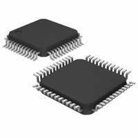
IC ADC 14BIT 8CH 2MSPS 48LQFP
Manufacturer
Maxim Integrated Products
Datasheet
1.MAX1318ECM.pdf
(27 pages)
Specifications of MAX1320ECM+
Number Of Bits
14
Sampling Rate (per Second)
2M
Data Interface
Parallel
Number Of Converters
1
Power Dissipation (max)
1.82W
Voltage Supply Source
Analog and Digital
Operating Temperature
-40°C ~ 85°C
Mounting Type
Surface Mount
Package / Case
48-LQFP
Lead Free Status / RoHS Status
Lead free / RoHS Compliant


8-/4-/2-Channel, 14-Bit, Simultaneous-Sampling ADCs
with ±10V, ±5V, and 0 to +5V Analog Input Ranges
10
MAX1316
MAX1320
MAX1324
______________________________________________________________________________________
10
11
12
13
18
19
20
21
22
24
25
26
MAX1317
MAX1321
MAX1325
PIN
13
18
19
20
21
22
24
25
26
—
—
—
MAX1318
MAX1322
MAX1326
—
—
—
13
18
19
20
21
22
24
25
26
INTCLK/
EXTCLK
REF
NAME
REF+
COM
REF-
CH5
CH6
CH7
REF
D0
D1
D2
MS
Channel 5 Analog Input
Channel 6 Analog Input
Channel 7 Analog Input
Clock-Mode Select Input. Use INTCLK/EXTCLK to select the internal
or external conversion clock. Connect INTCLK/EXTCLK to AV
select the internal clock. Connect INTCLK/EXTCLK to AGND to use
an external clock connected to CLK.
Midscale Reference Bypass or Input. REF
an internally generated reference voltage. For the MAX1316/
MAX1317/MAX1318, connect a 0.1µF capacitor from REF
AGND. For the MAX1320/MAX1321/MAX1322/MAX1324/
MAX1325/MAX1326, connect REF
with a 0.1µF capacitor from REF
ADC Reference Bypass or Input. REF is the bypass point for an
internally generated reference voltage. Bypass REF with a 0.01µF
capacitor to AGND. REF can be driven externally by a precision
external voltage reference.
Positive Reference Bypass. REF+ is the bypass point for an
internally generated reference voltage. Bypass REF+ with a 0.1µF
capacitor to AGND. Also bypass REF+ to REF- with a 2.2µF and a
0.1µF capacitor.
Reference Common Bypass. COM is the bypass point for an
internally generated reference voltage. Bypass COM to AGND with
a 2.2µF and a 0.1µF capacitor.
Negative Reference Bypass. REF- is the bypass point for an
internally generated reference voltage. Bypass REF- with a 0.1µF
capacitor to AGND. Also bypass REF- to REF+ with a 2.2µF and a
0.1µF capacitor.
Digital I/O Bit 0 of 14-Bit Parallel Data Bus. High impedance when
RD = 1 or CS = 1.
Digital I/O Bit 1 of 14-Bit Parallel Data Bus. High impedance when
RD = 1 or CS = 1.
Digital I/O Bit 2 of 14-Bit Parallel Data Bus. High impedance when
RD = 1 or CS = 1.
Pin Description (continued)
FUNCTION
MS
MS
to AGND.
directly to REF and bypass
MS
is the bypass point for
MS
to
DD
to
Related parts for MAX1320ECM+
Image
Part Number
Description
Manufacturer
Datasheet
Request
R

Part Number:
Description:
MAX7528KCWPMaxim Integrated Products [CMOS Dual 8-Bit Buffered Multiplying DACs]
Manufacturer:
Maxim Integrated Products
Datasheet:
Part Number:
Description:
Single +5V, fully integrated, 1.25Gbps laser diode driver.
Manufacturer:
Maxim Integrated Products
Datasheet:
Part Number:
Description:
Single +5V, fully integrated, 155Mbps laser diode driver.
Manufacturer:
Maxim Integrated Products
Datasheet:
Part Number:
Description:
VRD11/VRD10, K8 Rev F 2/3/4-Phase PWM Controllers with Integrated Dual MOSFET Drivers
Manufacturer:
Maxim Integrated Products
Datasheet:
Part Number:
Description:
Highly Integrated Level 2 SMBus Battery Chargers
Manufacturer:
Maxim Integrated Products
Datasheet:
Part Number:
Description:
Current Monitor and Accumulator with Integrated Sense Resistor; ; Temperature Range: -40°C to +85°C
Manufacturer:
Maxim Integrated Products
Part Number:
Description:
TSSOP 14/A�/RS-485 Transceivers with Integrated 100O/120O Termination Resis
Manufacturer:
Maxim Integrated Products
Part Number:
Description:
TSSOP 14/A�/RS-485 Transceivers with Integrated 100O/120O Termination Resis
Manufacturer:
Maxim Integrated Products
Part Number:
Description:
QFN 16/A�/AC-DC and DC-DC Peak-Current-Mode Converters with Integrated Step
Manufacturer:
Maxim Integrated Products
Part Number:
Description:
TDFN/A/65V, 1A, 600KHZ, SYNCHRONOUS STEP-DOWN REGULATOR WITH INTEGRATED SWI
Manufacturer:
Maxim Integrated Products
Part Number:
Description:
Integrated Temperature Controller f
Manufacturer:
Maxim Integrated Products
Part Number:
Description:
SOT23-6/I�/45MHz to 650MHz, Integrated IF VCOs with Differential Output
Manufacturer:
Maxim Integrated Products
Part Number:
Description:
SOT23-6/I�/45MHz to 650MHz, Integrated IF VCOs with Differential Output
Manufacturer:
Maxim Integrated Products
Part Number:
Description:
EVALUATION KIT/2.4GHZ TO 2.5GHZ 802.11G/B RF TRANSCEIVER WITH INTEGRATED PA
Manufacturer:
Maxim Integrated Products
Part Number:
Description:
QFN/E/DUAL PCIE/SATA HIGH SPEED SWITCH WITH INTEGRATED BIAS RESISTOR
Manufacturer:
Maxim Integrated Products
Datasheet: