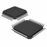
MAX1321ECM+ Maxim Integrated Products, MAX1321ECM+ Datasheet - Page 5

MAX1321ECM+
Manufacturer Part Number
MAX1321ECM+
Description
IC ADC 14BIT 4CH 1.4MSPS 48LQFP
Manufacturer
Maxim Integrated Products
Datasheet
1.MAX1318ECM.pdf
(27 pages)
Specifications of MAX1321ECM+
Number Of Bits
14
Sampling Rate (per Second)
1.4M
Data Interface
Parallel
Number Of Converters
1
Voltage Supply Source
Single Supply
Operating Temperature
-40°C ~ 85°C
Mounting Type
Surface Mount
Package / Case
48-LQFP
Lead Free Status / RoHS Status
Lead free / RoHS Compliant
TIMING CHARACTERISTICS (Figures 3, 4, 5, 6 and 7) (Tables 1, 3)
Note 1:
Note 2:
Note 3:
Note 4:
Note 5:
Note 6:
8-/4-/2-Channel, 14-Bit, Simultaneous-Sampling ADCs
Time-to-First-Conversion Result
Time-to-Next-Conversion Result
CONVST Pulse-Width Low
(Acquisition Time)
CS Pulse Width
RD Pulse-Width Low
RD Pulse-Width High
WR Pulse-Width Low
CS to WR
WR to CS
CS to RD
RD to CS
Data-Access Time
(RD Low to Valid Data)
Bus-Relinquish Time (RD High)
EOC Pulse Width
Input-Data Setup Time
Input-Data Hold Time
External-Clock Period
External-Clock High Period
External-Clock Low Period
External-Clock Frequency
Internal-Clock Frequency
CONVST High to CLK Edge
EOC Low to RD
with ±10V, ±5V, and 0 to +5V Analog Input Ranges
I
PARAMETER
For the MAX1316/MAX1317/MAX1318, V
MAX1324/MAX1325/MAX1326, V
All channel performance is guaranteed by correlation to a single channel test.
Offset nulled.
The analog input resistance is terminated to an internal bias point. Calculate the analog input current using:
for V
Throughput rate is given per channel. Throughput rate is a function of clock frequency (f
Throughput section for more information.
All analog inputs are driven with an FS 100kHz sine wave.
CH
_
CH
=
within the input voltage range.
V
_______________________________________________________________________________________
CH
_
R
CH
−
V
_
BIAS
SYMBOL
t
t
CONV
t
NEXT
ACQ
t
t
t
t
t
t
t
t
t
t
t
t
t
t
t
t
t
t
10
11
12
14
15
16
17
18
19
20
2
3
4
5
6
7
8
9
IN
= -10V to +10V.
Internal clock
External clock, Figure 6
Internal clock
External clock, Figure 6
(Note 9)
Internal clock
External clock, Figure 6
Logic sensitive to rising edges
Logic sensitive to rising edges
(Note 11)
IN
= 0 to +5V. For the MAX1320/MAX1321/MAX1322, V
CONDITIONS
0.16
0.08
MIN
0.1
30
30
30
30
80
10
10
20
20
20
CLK
(Note 10)
(Note 10)
(Note 10)
(Note 10)
(Note 12)
= 10MHz). See the Data
TYP
1.6
0.3
16
10
1
IN
3
0
= -5V to +5V. For the
10.00
MAX
0.36
12.5
100
1.8
30
30
UNITS
cycles
cycles
cycles
Clock
Clock
Clock
MHz
MHz
µs
µs
µs
ns
ns
ns
ns
ns
ns
ns
ns
ns
ns
ns
ns
ns
µs
ns
ns
ns
ns
5


