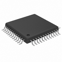
MAX1195ECM+TD Maxim Integrated Products, MAX1195ECM+TD Datasheet - Page 5

MAX1195ECM+TD
Manufacturer Part Number
MAX1195ECM+TD
Description
IC ADC 8BIT 40MSPS DL 48-TQFP
Manufacturer
Maxim Integrated Products
Datasheet
1.MAX1195ECMD.pdf
(22 pages)
Specifications of MAX1195ECM+TD
Number Of Bits
8
Sampling Rate (per Second)
40M
Data Interface
Parallel
Number Of Converters
2
Power Dissipation (max)
108mW
Voltage Supply Source
Single Supply
Operating Temperature
-40°C ~ 85°C
Mounting Type
Surface Mount
Package / Case
48-TQFP Exposed Pad, 48-eTQFP, 48-HTQFP, 48-VQFP
Lead Free Status / RoHS Status
Lead free / RoHS Compliant
ELECTRICAL CHARACTERISTICS (continued)
(V
resistor, V
otherwise noted. ≥+25°C guaranteed by production test, <+25°C guaranteed by design and characerization. Typical values are at
T
A
Input High Threshold
Input Low Threshold
Input Hysteresis
Input Leakage
Input Capacitance
DIGITAL OUTPUTS ( D7A–D0A, D7B–D0B)
Output Voltage Low
Output Voltage High
Three-State Leakage Current
Three-State Output Capacitance
POWER REQUIREMENTS
Analog Supply Voltage Range
Output Supply Voltage Range
Analog Supply Current
Output Supply Current
Analog Power Dissipation
Power-Supply
Rejection
DD
DIGITAL INPUTS (CLK, PD, OE, SLEEP, T/B)
= +25°C.)
= OV
Dual, 8-Bit, 40Msps, 3V, Low-Power ADC with
IN
DD
PARAMETER
= 2V
= 3V, 0.1µF and 2.2µF capacitors from REFP, REFN, and COM to GND; REFOUT connected to REFIN through a 10kΩ
P-P
_______________________________________________________________________________________
(differential with respect to COM), C
Internal Reference and Parallel Outputs
SYMBOL
V
PDISS
OV
I
C
PSRR
I
OVDD
V
I
LEAK
V
V
HYST
C
V
VDD
V
I
I
OUT
OH
DD
IH
OL
IL
IH
IL
IN
DD
CLK
PD, OE, SLEEP, T/B
CLK
PD, OE, SLEEP, T/B
V
V
I
I
OE = OV
OE = OV
C
Operating, f
-1dB FS applied to both channels
Sleep mode
Shutdown, clock idle, PD = OE = OV
Operating, f
-1dB FS applied to both channels (Note 6)
Sleep mode
Shutdown, clock idle, PD = OE = OV
Operating, f
-1dB FS applied to both channels
Sleep mode
Shutdown, clock idle, PD = OE = OV
Offset, V
Gain, V
SINK
SOURCE
IH
IL
L
= 15pF
= 0
= V
= -200µA
DD
DD
DD
DD
DD
= 200µA
L
= OV
±5%
= 10pF at digital outputs, f
INA & B
INA & B
INA & B
±5%
CONDITIONS
DD
= 20MHz at
= 20MHz at
= 20MHz at
DD
DD
DD
CLK
= 40MHz, T
OV
0.8 ×
0.8 ×
MIN
V
OV
2.7
1.7
- 0.2
DD
DD
DD
A
T YP
0.15
0.1
0.3
29
87
±3
±3
5
5
3
3
3
8
3
3
9
= T
MIN
OV
MAX
0.2 ×
0.2 ×
V
to T
±20
±20
±10
108
0.2
3.6
3.6
36
20
10
60
DD
DD
MAX
, unless
UNITS
mV/V
mW
mA
mA
µW
µA
pF
µA
pF
µA
µA
V
V
V
V
V
V
V
5


