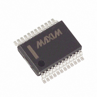
MAX113CAG+T Maxim Integrated Products, MAX113CAG+T Datasheet - Page 4

MAX113CAG+T
Manufacturer Part Number
MAX113CAG+T
Description
IC ADC 8BIT 400KSPS 24-SSOP
Manufacturer
Maxim Integrated Products
Datasheet
1.MAX113CAG.pdf
(12 pages)
Specifications of MAX113CAG+T
Number Of Bits
8
Sampling Rate (per Second)
400k
Data Interface
Parallel
Number Of Converters
3
Power Dissipation (max)
640mW
Voltage Supply Source
Single Supply
Operating Temperature
0°C ~ 70°C
Mounting Type
Surface Mount
Package / Case
24-SSOP
Lead Free Status / RoHS Status
Lead free / RoHS Compliant
+3V, 400ksps, 4/8-Channel,
8-Bit ADCs with 1µA Power-Down
TIMING CHARACTERISTICS
(V
Note 4: Input control signals are specified with t
Note 5: See Figure 1 for load circuit. Parameter defined as the time required for the output to cross 0.66V or 2.0V.
Note 6: See Figure 2 for load circuit. Parameter defined as the time required for the data lines to change 0.5V.
Note 7: Also defined as the Minimum Address-Valid to Convert-Start Time.
4
Conversion Time
(WR-RD Mode)
Conversion Time
(RD Mode)
Power-Up Time
CS to RD, WR
Setup Time
CS to RD, WR
Hold Time
CS to RDY Delay
Data Access Time
(RD Mode)
RD to INT Delay
(RD Mode)
Data Hold Time
Minimum
Acquisition Time
WR Pulse Width
Delay Between WR
and RD Pulses
RD Pulse Width
(WR-RD Mode)
Data Access Time
(WR-RD Mode)
RD to INT Delay
WR to INT Delay
RD Pulse Width
(WR-RD Mode)
Data Access Time
(WR-RD Mode)
WR to INT Delay
Data Access Time
After INT
Multiplexer Address
Hold Time
DD
_______________________________________________________________________________________
PARAMETER
= +3V, T
delays get shorter at higher supply voltages. See the Conversion Time vs. Supply Voltage graph in the Typical Operating
Characteristics to extrapolate timing delays at other power-supply voltages.
A
= +25°C, unless otherwise noted.) (Note 4)
SYMBOL
t
t
t
READ1
t
READ2
t
t
t
t
t
t
t
t
t
t
ACC0
ACC1
ACC2
IHWR
CWR
INTH
t
CRD
CSH
t
ACQ
t
INTL
t
t
CSS
RDY
WR
t
t
DH
RD
AH
UP
RI
ID
t
(Note 5)
C
R
C
C
(Note 6)
(Note 7)
t
t
t
(Note 5)
C
t
t
t
(Note 5)
Pipelined mode, C
Pipelined mode, C
RD
RD
ACC1
RD
RD
ACC2
RD
L
L
L
L
L
= 5.1kΩ to V
= 50pF,
= 100pF (Note 5)
= 50pF
= 50pF
< t
< t
< t
> t
> t
INTL
INTL
INTL
INTL
INTL
CONDITIONS
, C
, determined by
, C
, determined by
, C
r
L
L
L
= t
= 100pF
= 100pF
= 100pF
DD
f
= 5ns, 10% to 90% of 3V, and timed from a voltage level of 1.3V. Timing
L
L
= 50pF
= 100pF
MIN
450
400
180
0.6
0.8
50
0
0
ALL GRADES
T
A
TYP
100
= +25°C
0.7
t
CRD
MAX
1.45
100
100
160
100
400
300
180
180
100
1.8
2.0
0.9
10
+
0.66
MIN
600
500
220
0.9
60
MAX117C/E
0
0
T
A
t
CRD
MAX
2.06
= T
120
130
170
130
500
340
220
200
130
2.4
1.2
1.6
10
MIN
+
to T
MIN
700
600
250
0.8
1.0
70
0
0
MAX117M
MAX
t
CRD
MAX
140
150
180
150
600
400
250
240
150
2.4
2.6
1.4
1.8
10
+
UNITS
µs
µs
µs
ns
ns
ns
ns
ns
ns
ns
µs
µs
ns
ns
ns
µs
ns
ns
ns
ns
ns


