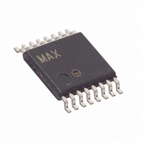
MAX1415EUE+T Maxim Integrated Products, MAX1415EUE+T Datasheet - Page 2

MAX1415EUE+T
Manufacturer Part Number
MAX1415EUE+T
Description
IC ADC 16BIT DELTA SIGMA 16TSSOP
Manufacturer
Maxim Integrated Products
Datasheet
1.MAX1415EUE.pdf
(36 pages)
Specifications of MAX1415EUE+T
Number Of Bits
16
Sampling Rate (per Second)
500
Data Interface
MICROWIRE™, QSPI™, Serial, SPI™
Number Of Converters
1
Power Dissipation (max)
755mW
Voltage Supply Source
Single Supply
Operating Temperature
-45°C ~ 85°C
Mounting Type
Surface Mount
Package / Case
16-TSSOP
Lead Free Status / RoHS Status
Lead free / RoHS Compliant
ABSOLUTE MAXIMUM RATINGS
V
All Other Pins to GND.................................-0.3V to (V
Maximum Current Input into Any Pin ..................................50mA
Continuous Power Dissipation (T
16-Bit, Low-Power, 2-Channel,
Sigma-Delta ADCs
Stresses beyond those listed under “Absolute Maximum Ratings” may cause permanent damage to the device. These are stress ratings only, and functional
operation of the device at these or any other conditions beyond those indicated in the operational sections of the specifications is not implied. Exposure to
absolute maximum rating conditions for extended periods may affect device reliability.
ELECTRICAL CHARACTERISTICS—MAX1415
(V
GND = 0.1µF, T
2
DC ACCURACY
Resolution (No Missing Codes)
Output Noise
Integral Nonlinearity
Unipolar Offset Error
Unipolar Offset Drift
Bipolar Zero Error
Bipolar Zero Drift (Note 2)
Positive Full-Scale Error
Full-Scale Drift
Gain Error
Gain Drift
Bipolar Negative Full-Scale Error
Bipolar Negative Full-Scale Drift
(Note 2)
ANALOG INPUTS (AIN1+, AIN1-, AIN2+, AIN2-)
AIN Differential Input Voltage
Range (Note 7)
AIN Absolute Input Voltage
Range (Note 8)
AIN DC Leakage Current
DD
DD
16-Pin PDIP (derate 10.5mW/°C above +70°C)...........842mW
16-Pin TSSOP (derate 9.4mW/°C above +70°C) .........755mW
16-Pin Wide SO (derate 9.5mW/°C above +70°C) ......762mW
_______________________________________________________________________________________
to GND ..............................................................-0.3V to +6V
= 3V, GND = 0, V
PARAMETER
A
= T
MIN
REF+
to T
= 1.225V, V
MAX
A
, unless otherwise noted.)
= +70°C)
SYMBOL
INL
REF-
= GND, external f
Gain = 1, bipolar mode, unbuffered
After calibration
(Note 2)
After calibration
Gain = 1 to 4
Gain = 8 to 128
After calibration
(Notes 2, 4)
After calibration
(Notes 2, 6)
After calibration
Gain = 1 to 4
Gain = 8 to 128
Unipolar input range
Bipolar input range
Unbuffered
Buffered
Unselected input channel
DD
+ 0.3V)
CLKIN
CONDITIONS
Operating Temperature Range ..........................-40°C to +85°C
Storage Temperature Range .............................-60°C to +150°C
Junction Temperature ......................................................+150°C
Lead Temperature (soldering, 10s) .................................+300°C
= 2.4576MHz, CLKDIV bit = 0, C
-V
GND +
GND -
30mV
50mV
GAIN
MIN
REF
16
0
/
REF+
(Tables 1, 3)
(Notes 1, 3)
(Notes 1, 5)
(Note 1)
(Note 1)
±0.003
TYP
0.5
0.5
0.1
0.5
0.5
0.6
to GND = 0.1µF, C
1
±0.0015
V
V
V
30mV
GAIN
GAIN
V
MAX
1.5V
REF
REF
DD
DD
1
+
-
/
/
FSR/°C
ppm of
UNITS
%FSR
%FSR
µV/°C
µV/°C
µV/°C
µV/°C
Bits
REF-
µV
µV
µV
µV
µV
nA
V
V
to


