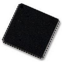
AD9262BCPZ-10 Analog Devices Inc, AD9262BCPZ-10 Datasheet - Page 19

AD9262BCPZ-10
Manufacturer Part Number
AD9262BCPZ-10
Description
IC ADC 16BIT 10MHZ 64LFCSP
Manufacturer
Analog Devices Inc
Datasheet
1.AD9262BCPZRL7.pdf
(32 pages)
Specifications of AD9262BCPZ-10
Data Interface
Serial, SPI™
Design Resources
Interfacing ADL5382 to AD9262 as an RF-to-Bits Solution (CN0062)
Number Of Bits
16
Sampling Rate (per Second)
160M
Number Of Converters
2
Power Dissipation (max)
762mW
Voltage Supply Source
Analog and Digital
Operating Temperature
-40°C ~ 85°C
Mounting Type
Surface Mount
Package / Case
64-LFCSP
Resolution (bits)
16bit
Sampling Rate
160MSPS
Input Channel Type
Differential, Single Ended
Supply Voltage Range - Analog
1.7V To 1.9V
Supply Current
146mA
Lead Free Status / RoHS Status
Lead free / RoHS Compliant
CLK+/CLK–
Internal PLL Clock Distribution
The alternative clocking option available on the AD9262 is to apply
a low frequency reference clock and use the on-chip clock multip-
lier to generate the high frequency f
architecture is shown in Figure 53.
The clock multiplication circuit operates such that the VCO
outputs a frequency, f
multiplied by N.
where N is the PLL multiplication (PLLMULT) factor.
The Σ-Δ modulator clock frequency, f
The reference clock, CLK±, is limited to 30 MHz to 160 MHz
when configured to use the on-chip clock multiplier. Given the
input range of the reference clock and the available multiplication
factors, the f
desired f
Before the PLL enable register bit (PLLENABLE) is set, the PLL
multiplication factor should be programmed into Register
0x0A[5:0]. After setting the PLLENABLE bit, the PLL locks and
reports a locked state in Register 0x0A[7]. If the PLL multiplica-
tion factor is changed, the PLL enable bit should be reset and set
again. Some common clock multiplication factors are shown in
Table 11.
The recommended sequence for enabling and programming the
on-chip clock multiplier is shown in Table 9.
Table 9. Sequence for Enabling and Programming the PLL
Step
1
2
3
4
5
6
f
f
MOD
VCO
MOD
= (CLK±) × (N)
= f
VCO
Procedure
Apply a reference clock to the CLK± pins.
Program the PLL multiplication factor in
Register 0x0A[5:0]. See Table 10.
Enable the PLL; Register 0x09 = 04 (decimal).
Enable PLL autoband select.
Initiate an SRC reset; Register 0x101[5:0] = 0.
Set SRC to desired value via Register 0x101[5:0].
VCO
rate of 640 MHz with a 50% duty cycle.
÷ 2
is approximately 1280 MHz. This results in the
Figure 53. Internal Clock Architecture
DETECTOR
PHASE
VCO
, equal to the reference clock input
PLL MULT
0x0A[5:0]
DIVIDER
FILTER
LOOP
MOD
MOD
rate. The internal clock
PLL
, is equal to
÷2
PLLENABLE
0x09[2]
VCO
MODULATOR
640MSPS
CLOCK
Rev. A | Page 19 of 32
PLL Autoband Select
The PLL VCO has a wide operating range that is covered by
overlapping frequency bands. For any desired VCO output
frequency, there are multiple valid PLL band select values. The
AD9262 possesses an automatic PLL band select feature on chip
that determines the optimal PLL band setting. This feature can
be enabled by writing to Register 0x0A[6]and is the recommended
configuration with the PLL clocking option. When the device is
taken out of sleep or standby mode, Register 0x0A[6] must be
toggled to reinitiate the autoband detect. See Table 9 for informa-
tion about enabling the autoband select along with configuring
the PLL.
Table 10. PLL Multiplication Factors
0x0A[5:0]
1
2
3
4
5
6
7
8
9
10
11
12
13
14
15
16
17
18
19
20
21
22
23
24
25
26
27
28
29
30
31
32
PLLMULT (N)
8
8
8
8
8
8
8
8
9
10
10
12
12
14
15
16
17
18
18
20
21
21
21
24
25
25
25
28
28
30
30
32
0x0A[5:0]
33
34
35
36
37
38
39
40
41
42
43
44
45
46
47
48
49
50
51
52
53
54
55
56
57
58
59
60
61
62
63
64
PLLMULT (N)
32
34
34
34
34
34
34
34
34
42
42
42
42
42
42
42
42
42
42
42
42
42
42
42
42
42
42
42
42
42
42
42
AD9262


