AD9058AJJ Analog Devices Inc, AD9058AJJ Datasheet - Page 6
AD9058AJJ
Manufacturer Part Number
AD9058AJJ
Description
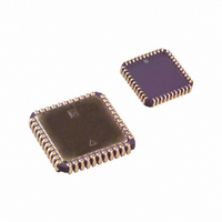
IC ADC 8BIT DUAL 50MSPS 44-JLCC
Manufacturer
Analog Devices Inc
Datasheet
1.AD9058AJJ.pdf
(12 pages)
Specifications of AD9058AJJ
Data Interface
Parallel
Rohs Status
RoHS non-compliant
Number Of Bits
8
Sampling Rate (per Second)
50M
Number Of Converters
2
Power Dissipation (max)
960mW
Voltage Supply Source
Analog and Digital, Dual ±
Operating Temperature
0°C ~ 70°C
Mounting Type
Surface Mount
Package / Case
44-JLCC
Resolution (bits)
8bit
Sampling Rate
50MSPS
Input Channel Type
Single Ended
Supply Voltage Range - Analog
± 5V
Supply Current
127mA
Digital Ic Case Style
JLCC
Lead Free Status / RoHS Status
Contains lead / RoHS non-compliant
Available stocks
Company
Part Number
Manufacturer
Quantity
Price


AD9058
THEORY OF OPERATION
The AD9058 contains two separate 8-bit analog-to-digital con-
verters (ADCs) on a single silicon die. The two devices can be
operated independently with separate analog inputs, voltage
references, and clocks.
In a traditional flash converter, 256 input comparators are required
to make the parallel conversion for 8-bit resolution. This is in
marked contrast to the scheme used in the AD9058, as shown
in Figure 1.
Unlike traditional “flash,” or parallel, converters, each of the two
ADCs in the AD9058 utilizes a patented interpolating archi-
tecture to reduce circuit complexity, die size, and input capacitance.
These advantages accrue because, compared to a conventional
flash design, only half the normal number of input comparator
cells is required to accomplish the conversion.
In this unit, each of the two independent ADCs uses only 128 (2
comparators to make the conversion. The conversion for the
seven most significant bits (MSBs) is performed by the 128
comparators. The value of the least significant bit (LSB) is
determined by interpolation between adjacent comparators in
the decoding register. A proprietary decoding scheme processes
the comparator outputs and provides an 8-bit code to the output
register of each ADC; the scheme also minimizes error codes.
IN A
IN B
ANALOG
ANALOG
0.5V
0.5V
0.1 F
200
200
800
–2V
800
AD9617
400
20k
AD9617
Figure 2. AD9058 Using Internal 2 V Voltage Reference
400
AD707
20k
0.1 F
5
5
0.1 F
+2V
ENCODE
38
43
40
7
8
6
2
3
1
)
–6–
–V
–V
COMP
AD9058
(J-LEAD)
A
+V
+V
+V
A
IN A
IN B
ENCODE
REF A
REF B
REF A
REF B
INT
10
Analog input range is established by the voltages applied at the
voltage reference inputs (+V
operate from 0 V to 2 V using the internal voltage reference,
or anywhere between –1 V and +2 V using external references.
Input range is limited to 2 V p-p when using external references.
The internal resistor ladder divides the applied voltage reference
into 128 steps, with each step representing two 8-bit quanti-
zation levels.
A
4, 19, 21,
25, 27, 42
ANALOG IN
–V
+V
REF
REF
ENCODE
36
D
D
D
D
7A
7B
B
0A
0B
Figure 1. Comparator Block Diagram
(MSB)
(MSB)
(LSB)
(LSB)
+V
–V
S
S
50
18
17
16
15
14
13
12
11
5, 9, 22,
24, 37, 41
28
29
30
31
32
33
34
35
7, 20,
26, 39
0.1 F
128
127
2
1
74HCT04
REF
1N4001
and –V
+5V
256
1k
–5V
REF
(SEE TEXT)
). The AD9058 can
8
10pF
CLOCK
CLOCK
8
8
REV. D
8
Related parts for AD9058AJJ
Image
Part Number
Description
Manufacturer
Datasheet
Request
R

Part Number:
Description:
±1.7g Dual-Axis IMEMS Accelerometer Evaluation Board
Manufacturer:
Analog Devices Inc
Datasheet:

Part Number:
Description:
Inertial Sensor Evaluation System
Manufacturer:
Analog Devices Inc
Datasheet:
Part Number:
Description:
Manufacturer:
Analog Devices Inc
Datasheet:
Part Number:
Description:
Manufacturer:
Analog Devices Inc
Datasheet:
Part Number:
Description:
Manufacturer:
Analog Devices Inc
Datasheet:
Part Number:
Description:
Manufacturer:
Analog Devices Inc
Datasheet:
Part Number:
Description:
Manufacturer:
Analog Devices Inc
Datasheet:
Part Number:
Description:
Manufacturer:
Analog Devices Inc
Datasheet:
Part Number:
Description:
Manufacturer:
Analog Devices Inc
Datasheet:
Part Number:
Description:
Manufacturer:
Analog Devices Inc
Datasheet:
Part Number:
Description:
Manufacturer:
Analog Devices Inc
Datasheet:
Part Number:
Description:
Manufacturer:
Analog Devices Inc
Datasheet:
Part Number:
Description:
Manufacturer:
Analog Devices Inc
Datasheet: