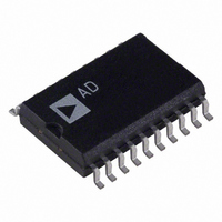
AD977BR Analog Devices Inc, AD977BR Datasheet - Page 12

AD977BR
Manufacturer Part Number
AD977BR
Description
IC ADC 16BIT 100KSPS 20-SOIC
Manufacturer
Analog Devices Inc
Datasheet
1.AD977ARZ.pdf
(24 pages)
Specifications of AD977BR
Data Interface
Serial, SPI™
Rohs Status
RoHS non-compliant
Number Of Bits
16
Sampling Rate (per Second)
100k
Number Of Converters
1
Power Dissipation (max)
100mW
Voltage Supply Source
Analog and Digital
Operating Temperature
-40°C ~ 85°C
Mounting Type
Surface Mount
Package / Case
20-SOIC (0.300", 7.50mm Width)
Resolution (bits)
16bit
Sampling Rate
100kSPS
Input Channel Type
Single Ended
Supply Voltage Range - Analog
4.75V To 5.25V
Supply Voltage Range - Digital
4.75V To 5.25V
For Use With
EVAL-AD977CB - BOARD EVAL FOR AD977EVAL-AD977ACB - BOARD EVAL FOR AD977A
Lead Free Status / RoHS Status
Contains lead / RoHS non-compliant
Available stocks
Company
Part Number
Manufacturer
Quantity
Price
Part Number:
AD977BR
Manufacturer:
ADI/亚德诺
Quantity:
20 000
Part Number:
AD977BRS
Manufacturer:
ADI/亚德诺
Quantity:
20 000
Part Number:
AD977BRSZ
Manufacturer:
ADI/亚德诺
Quantity:
20 000
Company:
Part Number:
AD977BRZ
Manufacturer:
AD
Quantity:
3 020
Part Number:
AD977BRZ
Manufacturer:
ADI/亚德诺
Quantity:
20 000
Part Number:
AD977BRZRL
Manufacturer:
ADI/亚德诺
Quantity:
20 000
AD977/AD977A
For both the AD977 and the AD977A the data should be
clocked out during the first half of BUSY so not to degrade
conversion performance. For the AD977 this requires use of a
4.8 MHz DATACLK or greater, with data being read out as
soon as the conversion process begins. For the AD977A it
requires use of a 10 MHz DATACLK or greater.
It is not recommended that data be shifted through the TAG
input in this mode as it will certainly result in clocking of data
during the second half of the conversion.
EXTERNAL CONTINUOUS CLOCK DATA READ AFTER
CONVERSION WITH SYNC OUTPUT GENERATED
Figure 8 illustrates the method by which data from conversion
“n” can be read after the conversion is complete using a con-
tinuous external clock, with the generation of a SYNC output.
What permits the generation of a SYNC output is a transition of
DATACLK while either CS is high or while both CS and R/C are
low.
With a continuous clock the CS pin cannot be tied low as it
could be with a discontinuous clock. Use of a continuous clock,
while a conversion is occurring, can increase the DNL and
Transition Noise of the AD977/AD977A.
DATACLK
DATA
BUSY
SYNC
TAG
EXT
R/C
CS
t
16
t
t
1
2
t
13
0
t
16
t
t
12
17
t
14
1
t
15
t
t
TAG 0
23
12
t
t
24
18
2
TAG 1
BIT 15
(MSB)
3
After a conversion is complete, indicated by BUSY returning
high, the result of that conversion can be read while CS is low
and R/C is high. In Figure 8 clock pulse #0 is used to enable the
generation of a SYNC pulse. The SYNC pulse is actually clocked
out approximately 40 ns after the rising edge of clock pulse #1.
The SYNC pulse will be valid on the falling edge of clock pulse
#1 and the rising edge of clock pulse #2. The MSB will be valid
on the falling edge of clock pulse #2 and the rising edge of clock
pulse #3. The LSB will be valid on the falling edge of clock
pulse #17 and the rising edge of clock pulse #18. Approximately
50 ns after the rising edge of clock pulse #18 the DATA output
pin will reflect the state of the TAG input pin during the rising
edge of clock pulse #2.
When reading data after the conversion is complete, with the
highest frequency permitted for DATACLK (15.15 MHz) and,
with the AD977A, the maximum possible throughput is approxi-
mately 195 kHz and not the rated 200 kHz.
For details on use of the TAG input with this mode see the Use
of the TAG Input section.
BIT 14
TAG 2
4
17
TAG 16
(LSB)
BIT 0
18
t
18
INT
TAG 0
TAG 17
t
19
TAG 1
TAG 18
TAG 2
TAG 19


